SNVS606L June 2009 – December 2014 LM3530
PRODUCTION DATA.
- 1 Features
- 2 Applications
- 3 Description
- 4 Revision History
- 5 I2C Device Options
- 6 Pin Configuration and Functions
- 7 Specifications
-
8 Detailed Description
- 8.1 Overview
- 8.2 Functional Block Diagram
- 8.3
Feature Description
- 8.3.1 Start-Up
- 8.3.2 Light Load Operation
- 8.3.3 Ambient Light Sensor
- 8.3.4 ALS Operation
- 8.3.5 ALS Averaging Time
- 8.3.6 Zone Boundary Settings
- 8.3.7 Zone Boundary Trip Points and Hysteresis
- 8.3.8 Minimum Zone Boundary Settings
- 8.3.9 LED Current Control
- 8.3.10 Exponential or Linear Brightness Mapping Modes
- 8.3.11 PWM Input Polarity
- 8.3.12 I2C-Compatible Current Control Only
- 8.3.13 Simple Enable Disable With PWM Current Control
- 8.3.14 Ambient Light Current Control
- 8.3.15 Ambient Light Current Control + PWM
- 8.3.16 Interrupt Output
- 8.3.17 Overvoltage Protection
- 8.3.18 Hardware Enable
- 8.3.19 Thermal Shutdown
- 8.4 Device Functional Modes
- 8.5 Programming
- 8.6 Register Maps
- 9 Application and Implementation
- 10Power Supply Recommendations
- 11Layout
- 12Device and Documentation Support
- 13Mechanical, Packaging, and Orderable Information
Package Options
Mechanical Data (Package|Pins)
Thermal pad, mechanical data (Package|Pins)
Orderable Information
6 Pin Configuration and Functions
DSBGA (YFZ or YFQ) Package
12 Pins
Top View
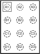
Pin Functions
| PIN | TYPE | DESCRIPTION | |
|---|---|---|---|
| NUMBER | NAME | ||
| A1 | SDA | I/O | Serial data connection for I2C-compatible interface. |
| A2 | SCL | I | Serial data connection for I2C-compatible interface. |
| A3 | SW | PWR | Inductor connection, diode anode connection, and drain connection for internal NFET. Connect the inductor and diode as close as possible to SW to reduce parasitic inductance and capacitive coupling to nearby traces. |
| B1 | PWM | I | External PWM brightness control input and simple enable input. |
| B2 | INT | O | Logic interrupt output signaling the ALS zone has changed. |
| B3 | GND | Ground | |
| C1 | ALS2 | I | Ambient light sensor input 2 with programmable internal pull-down resistor. |
| C2 | HWEN | I | Active high hardware enable (active low reset). pull this pin high to enable the LM3530. |
| C3 | IN | PWR | Input voltage connection. Connect a 2.7-V to 5.5-V supply to IN and bypass to GND with a 2.2-µF or greater ceramic capacitor. |
| D1 | ALS1 | I | Ambient light sensor input 1 with programmable internal pulldown resistor. |
| D2 | OVP | I | Output voltage sense connection for overvoltage sensing. Connect OVP to the positive terminal of the output capacitor. |
| D3 | ILED | PWR | Input terminal to internal current sink. The boost converter regulates ILED to 0.4 V. |