SNVS624B June 2011 – June 2016 LM3559
PRODUCTION DATA.
- 1 Features
- 2 Applications
- 3 Description
- 4 Revision History
- 5 Pin Configuration and Functions
- 6 Specifications
- 7 Typical Characteristics
-
8 Detailed Description
- 8.1 Overview
- 8.2 Functional Block Diagram
- 8.3
Feature Description
- 8.3.1 Power Amplifier Synchronization (TX1)
- 8.3.2 Input Voltage Flash Monitor Fault
- 8.3.3 Independent LED Control
- 8.3.4 Hardware Torch
- 8.3.5 Fault Protections
- 8.3.6 Input Voltage (VIN ) Monitor
- 8.3.7 VIN Flash Monitor (Flash Current Rising)
- 8.3.8 Last Flash Register
- 8.3.9 LED Voltage Monitor
- 8.3.10 ADC Delay
- 8.3.11 Flags Register and Fault Indicators
- 8.4
Device Functional Modes
- 8.4.1 Start-Up (Enabling the Device)
- 8.4.2 Pass Mode
- 8.4.3 Flash Mode
- 8.4.4 Torch Mode
- 8.4.5 Privacy-Indicate Mode
- 8.4.6 GPIO1 Mode
- 8.4.7 TX2/INT/GPIO2
- 8.4.8 TX2 Mode
- 8.4.9 GPIO2 Mode
- 8.4.10 Interrupt Output (INT Mode)
- 8.4.11 NTC Mode
- 8.4.12 Alternate External Torch (AET Mode)
- 8.4.13 Automatic Conversion Mode
- 8.4.14 Manual Conversion Mode
- 8.5 Programming
- 8.6
Register Maps
- 8.6.1 Enable Register
- 8.6.2 Torch Brightness Register
- 8.6.3 Flash Brightness Register
- 8.6.4 Flash Duration Register
- 8.6.5 Flags Register
- 8.6.6 Configuration Register 1
- 8.6.7 Configuration Register 2
- 8.6.8 GPIO Register
- 8.6.9 Last Flash Register
- 8.6.10 VLED Monitor Register
- 8.6.11 ADC Delay Register
- 8.6.12 Input Voltage Monitor Register
- 8.6.13 Privacy Register
- 8.6.14 Privacy PWM Period Register
- 8.6.15 Indicator Register
- 8.6.16 Indicator Blinking Register
- 9 Application and Implementation
- 10Power Supply Recommendations
- 11Layout
- 12Device and Documentation Support
- 13Mechanical, Packaging, and Orderable Information
Package Options
Mechanical Data (Package|Pins)
- YZR|16
Thermal pad, mechanical data (Package|Pins)
Orderable Information
1 Features
- Dual High-Side Current Sources Allow for Grounded Cathode LED Operation
- Accurate and Programmable LED Current from 28.125 mA to 1.8 A
- Optimized Flash Current During Low Battery Conditions
- Independent LED Current Source Programmability
- Four Operating Modes: Torch, Flash, Privacy Indicate, and Message Indicator
- 4-Bit Analog-to-Digital (ADC) for VLED Monitoring
- Battery Voltage Sensing and Current Scale-Back
- LED Sensing and Current Scale-Back
- Hardware Flash and Torch Enable
- Active-Low Hardware Reset
- Dual Synchronization Inputs for RF Power Amplifier Pulse Events
- LED and Output Disconnect During Shutdown
- Open and Short LED Detection
- 400-kHz I2C-Compatible Interface
2 Applications
- Camera Phone LED Flash
- White LED Biasing
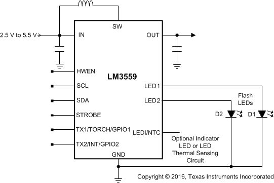
Simplified Schematic

3 Description
The LM3559 is a 2-MHz fixed-frequency synchronous boost converter with two 900-mA constant current drivers for high-current white LEDs. The dual high-side current sources allow for grounded cathode LED operation and can be tied together for providing flash currents of up to 1.8 A. An adaptive regulation method ensures the current for each LED remains in regulation and maximizes efficiency.
The LM3559 is controlled via an I2C-compatible interface. Features include: an internal 4-bit ADC to monitor the LED voltage, independent LED current control, a hardware flash enable allowing a logic input to trigger the flash pulse, dual TX inputs which force the flash pulse into a low-current torch mode allowing for synchronization to RF power amplifier events or other high-current conditions, an integrated comparator designed to monitor an NTC thermistor and provide an interrupt to the LED current, an input voltage monitor to monitor low battery conditions, and a flash current scale-back feature that actively monitors the battery voltage and optimizes the flash current during low battery-voltage conditions. Additionally, an active high HWEN input provides a hardware shutdown during system software failures.
The 2-MHz switching frequency, overvoltage protection, and adjustable current limit allow for the use of tiny, low-profile (1-µH or 2.2-µH) inductors and (10-µF) ceramic capacitors. The device is available in a ultra-small 16-pin DSBGA package (total solution size < 26 mm2) and operates over the –40°C to +85°C temperature range.
Device Information(1)
| PART NUMBER | PACKAGE | BODY SIZE (NOM) |
|---|---|---|
| LM3559 | DSBGA (16) | 1.96 mm × 1.96 mm |
- For all available packages, see the orderable addendum at the end of the data sheet.
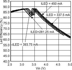
LED Efficiency vs VIN Dual LEDs

4 Revision History
Changes from A Revision (May 2013) to B Revision
- Added Device Information and Pin Configuration and Functions sections, ESD Ratings and Thermal Information tables, Feature Description, Device Functional Modes, Application and Implementation, Power Supply Recommendations, Layout, Device and Documentation Support, and Mechanical, Packaging, and Orderable Information sectionsGo
- Added Thermal Information table with revised RθJA value (from "50.4°C/W" to "71.3°C/W") and additional thermal values. Go
Changes from * Revision (May 2013) to A Revision
- Changed layout of National Data Sheet to TI formatGo