SNVS624B June   2011  – June 2016 LM3559

PRODUCTION DATA.  

  1. Features
  2. Applications
  3. Description
  4. Revision History
  5. Pin Configuration and Functions
  6. Specifications
    1. 6.1 Absolute Maximum Ratings
    2. 6.2 ESD Ratings
    3. 6.3 Recommended Operating Conditions
    4. 6.4 Thermal Information
    5. 6.5 Electrical Characteristics
    6. 6.6 I2C Timing Requirements (SCL, SDA)
  7. Typical Characteristics
  8. Detailed Description
    1. 8.1 Overview
    2. 8.2 Functional Block Diagram
    3. 8.3 Feature Description
      1. 8.3.1  Power Amplifier Synchronization (TX1)
      2. 8.3.2  Input Voltage Flash Monitor Fault
      3. 8.3.3  Independent LED Control
      4. 8.3.4  Hardware Torch
      5. 8.3.5  Fault Protections
        1. 8.3.5.1 Overvoltage Protection
        2. 8.3.5.2 Current Limit
        3. 8.3.5.3 Flash Timeout
        4. 8.3.5.4 Indicator LED/Thermistor (LEDI/NTC)
          1. 8.3.5.4.1 Message Indicator Current Source (LEDI/NTC)
            1. 8.3.5.4.1.1 Message Indicator Example 1 (Single Pulse With Dead Time):
            2. 8.3.5.4.1.2 Message Indicator Example 2 (Multiple Pulses With Dead Time):
            3. 8.3.5.4.1.3 Updating The Message Indicator
      6. 8.3.6  Input Voltage (VIN ) Monitor
      7. 8.3.7  VIN Flash Monitor (Flash Current Rising)
      8. 8.3.8  Last Flash Register
      9. 8.3.9  LED Voltage Monitor
      10. 8.3.10 ADC Delay
      11. 8.3.11 Flags Register and Fault Indicators
        1. 8.3.11.1 Flash Timeout
        2. 8.3.11.2 Thermal Shutdown
        3. 8.3.11.3 LED Fault
        4. 8.3.11.4 TX1 and TX2 Interrupt Flags
        5. 8.3.11.5 LED Thermal Fault (NTC Flag)
        6. 8.3.11.6 Input Voltage Monitor Fault
    4. 8.4 Device Functional Modes
      1. 8.4.1  Start-Up (Enabling the Device)
      2. 8.4.2  Pass Mode
      3. 8.4.3  Flash Mode
      4. 8.4.4  Torch Mode
      5. 8.4.5  Privacy-Indicate Mode
      6. 8.4.6  GPIO1 Mode
      7. 8.4.7  TX2/INT/GPIO2
      8. 8.4.8  TX2 Mode
        1. 8.4.8.1 TX2 Shutdown
      9. 8.4.9  GPIO2 Mode
      10. 8.4.10 Interrupt Output (INT Mode)
      11. 8.4.11 NTC Mode
      12. 8.4.12 Alternate External Torch (AET Mode)
      13. 8.4.13 Automatic Conversion Mode
      14. 8.4.14 Manual Conversion Mode
    5. 8.5 Programming
      1. 8.5.1 I2C-Compatible Interface
        1. 8.5.1.1 START and STOP Conditions
        2. 8.5.1.2 I2C-Compatible Chip Address
        3. 8.5.1.3 Transferring Data
    6. 8.6 Register Maps
      1. 8.6.1  Enable Register
      2. 8.6.2  Torch Brightness Register
      3. 8.6.3  Flash Brightness Register
      4. 8.6.4  Flash Duration Register
      5. 8.6.5  Flags Register
      6. 8.6.6  Configuration Register 1
      7. 8.6.7  Configuration Register 2
      8. 8.6.8  GPIO Register
      9. 8.6.9  Last Flash Register
      10. 8.6.10 VLED Monitor Register
      11. 8.6.11 ADC Delay Register
      12. 8.6.12 Input Voltage Monitor Register
      13. 8.6.13 Privacy Register
      14. 8.6.14 Privacy PWM Period Register
      15. 8.6.15 Indicator Register
      16. 8.6.16 Indicator Blinking Register
  9. Application and Implementation
    1. 9.1 Application Information
    2. 9.2 Typical Applications
      1. 9.2.1 LM3559 Typical Application
        1. 9.2.1.1 Design Requirements
        2. 9.2.1.2 Detailed Design Procedure
          1. 9.2.1.2.1 Output Capacitor Selection
          2. 9.2.1.2.2 Input Capacitor Selection
          3. 9.2.1.2.3 Inductor Selection
        3. 9.2.1.3 Application Curves
      2. 9.2.2 LM3559 Typical Application Circuit With Thermistor
        1. 9.2.2.1 Detailed Design Procedure
          1. 9.2.2.1.1 NTC Thermistor Selection
  10. 10Power Supply Recommendations
  11. 11Layout
    1. 11.1 Layout Guidelines
    2. 11.2 Layout Example
  12. 12Device and Documentation Support
    1. 12.1 Device Support
      1. 12.1.1 Third-Party Products Disclaimer
    2. 12.2 Documentation Support
      1. 12.2.1 Related Documentation
    3. 12.3 Receiving Notification of Documentation Updates
    4. 12.4 Community Resources
    5. 12.5 Trademarks
    6. 12.6 Electrostatic Discharge Caution
    7. 12.7 Glossary
  13. 13Mechanical, Packaging, and Orderable Information

Package Options

Mechanical Data (Package|Pins)
Thermal pad, mechanical data (Package|Pins)
Orderable Information

7 Typical Characteristics

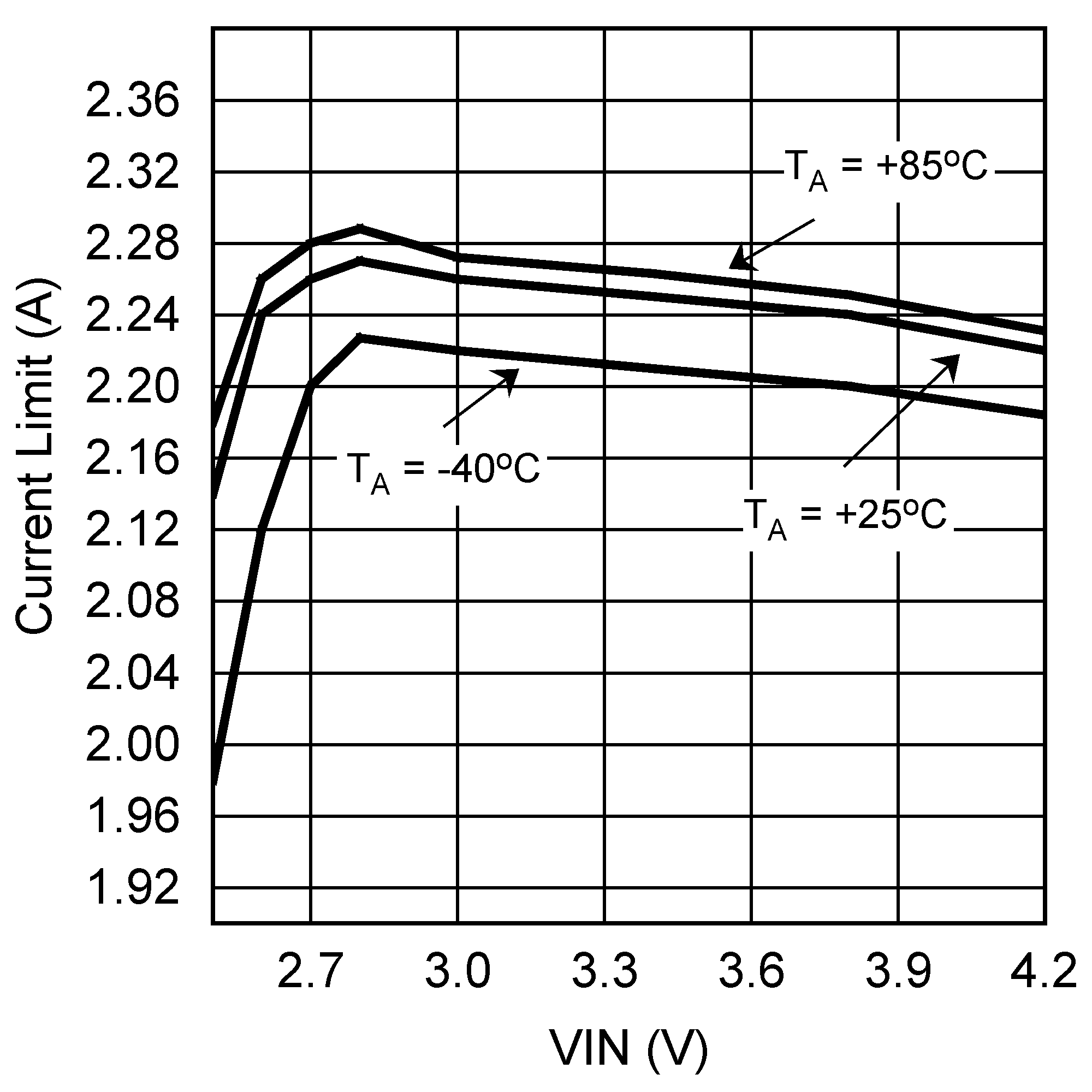
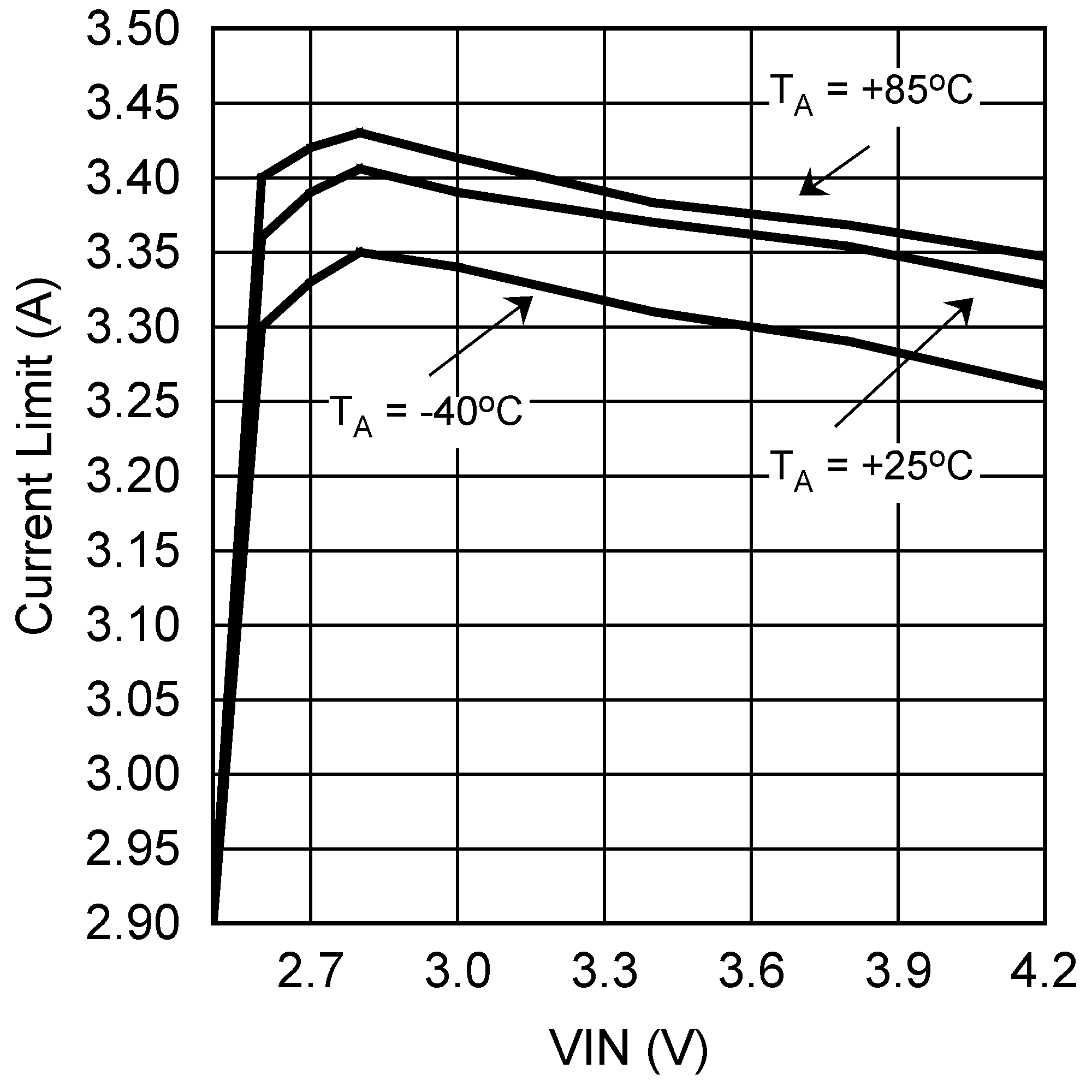
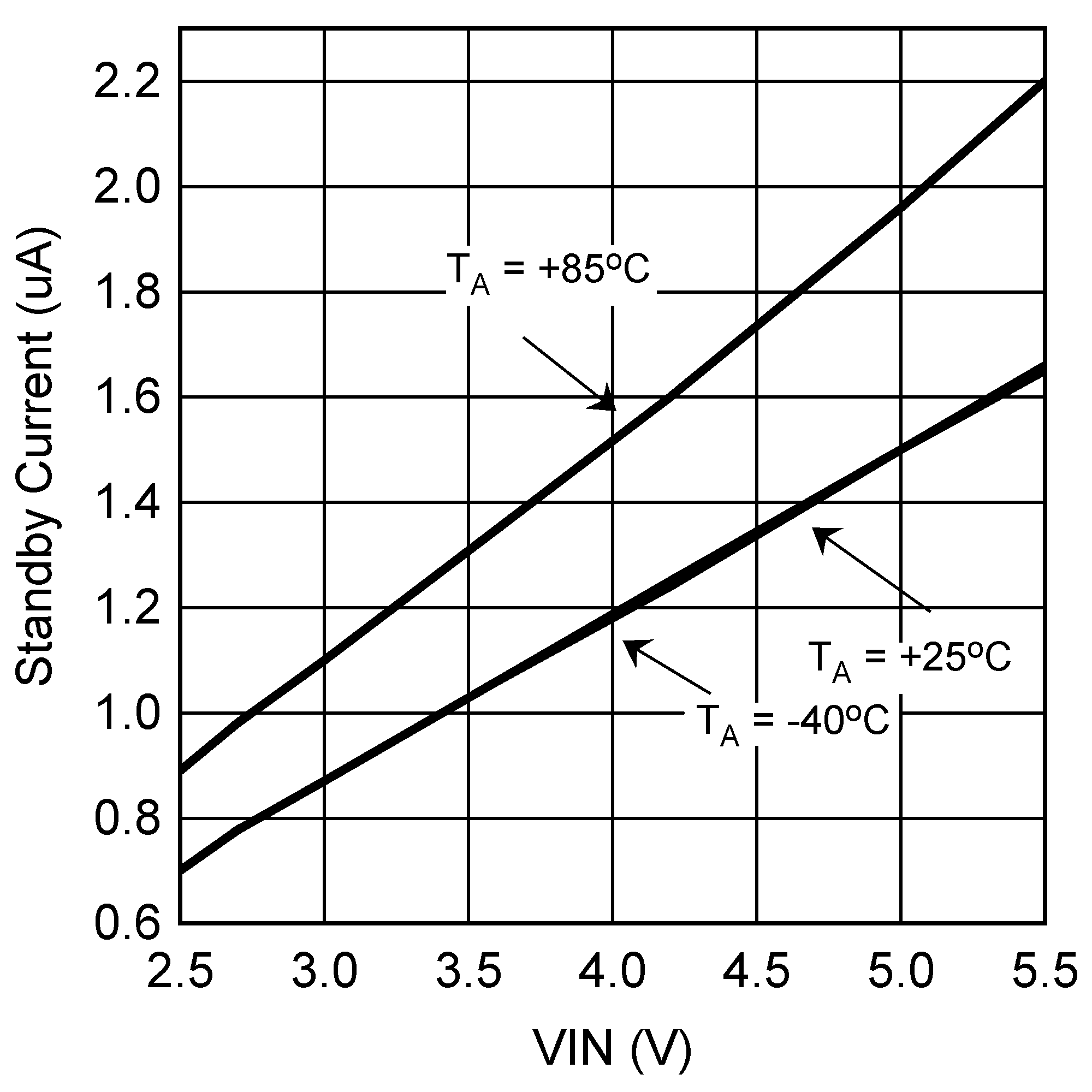
Unless otherwise specified: VIN = 3.6 V, COUT = 10 µF, CIN = 10 µF, L = 1 µH (TOKO FDSD0312-1R0, RL = 43 mΩ), Figure 43.
LM3559 30102885.png
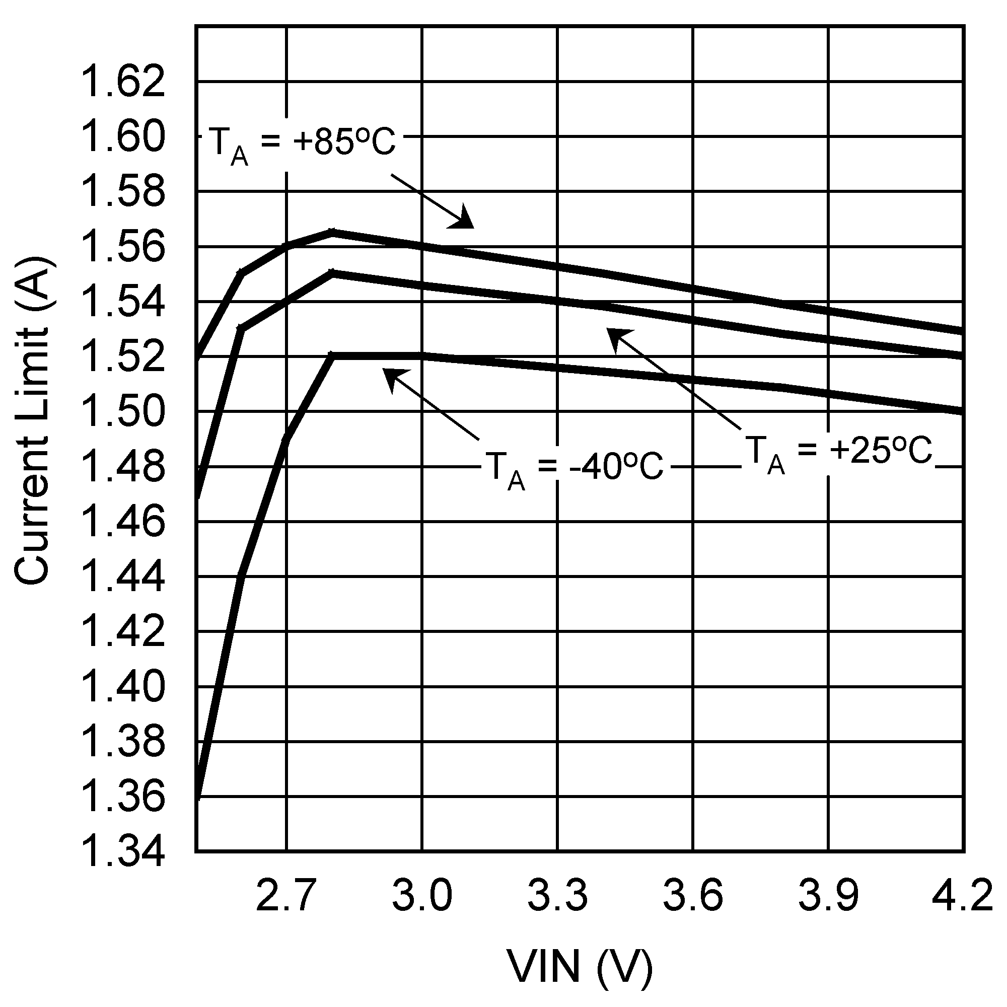
Register Bits [6:5] = 00
Figure 1. Closed Loop Current Limit vs VIN Flash Duration1
LM3559 30102887.png
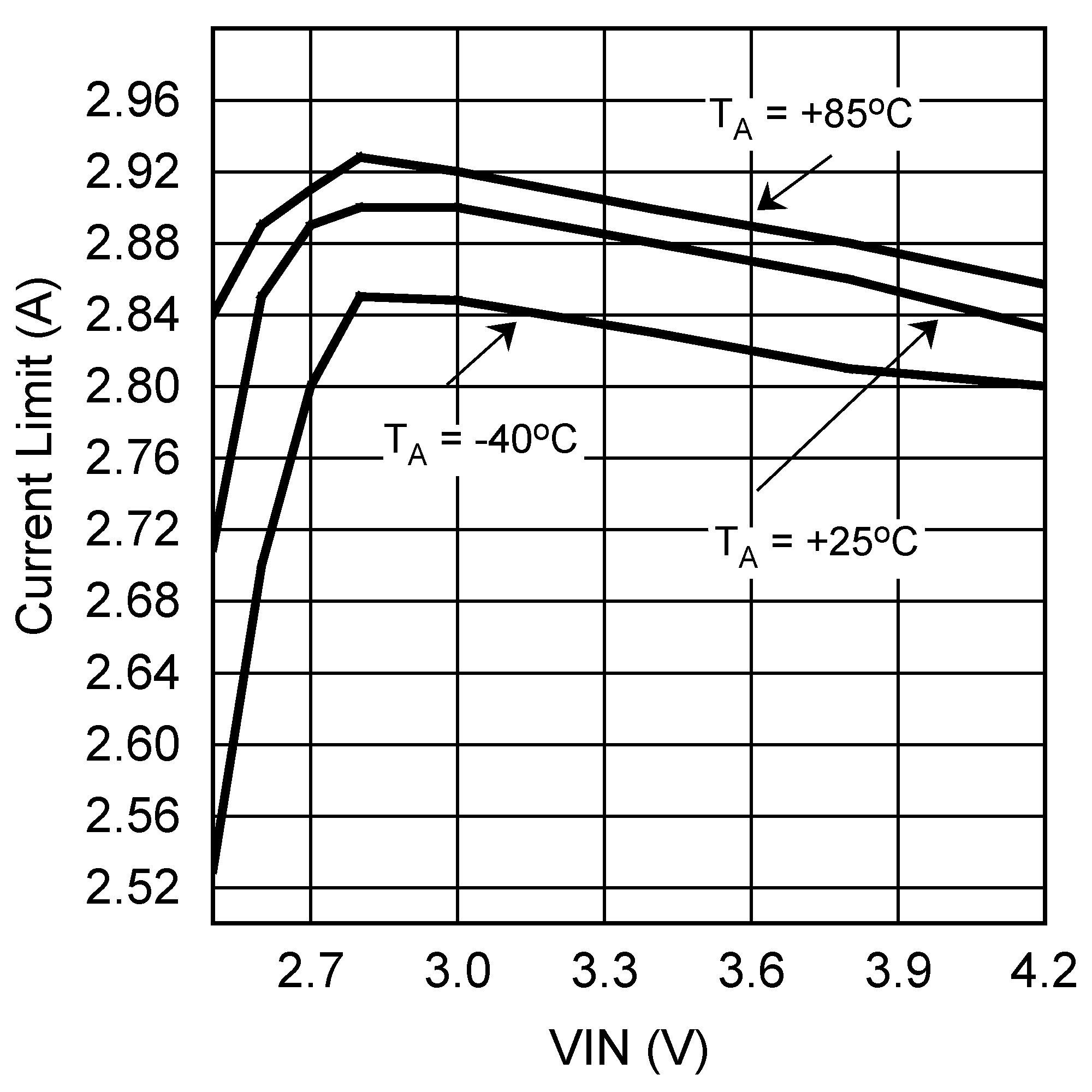
Register Bits [6:5] = 10
Figure 3. Closed Loop Current Limit vs VIN Flash Duration1
LM3559 30102897.png
Enable Register = 0x18
Figure 5. Standby Current vs VIN VHWEN = VIN
LM3559 30102861.gif
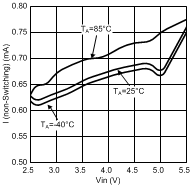
Figure 7. Non-Switching Current vs VIN
LM3559 30102863.gif
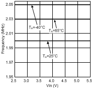
Figure 9. Switching Frequency vs VIN
LM3559 30102868.gif
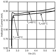
Register Bits [2:0] = 0x02
Figure 11. Indicator Current vs VIN Indicator
LM3559 30102872.gif
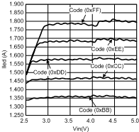
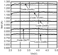
Upper 5 Flash Brightness Codes
Figure 13. ILED (Flash Mode) vs VIN LED1 and LED2 Connected Together
LM3559 30102874.gif
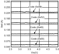
Upper 4 Torch Brightness Codes
Figure 15. ILED (Torch Mode) vs VIN LED1 and LED2 Connected Together
LM3559 30102877.png
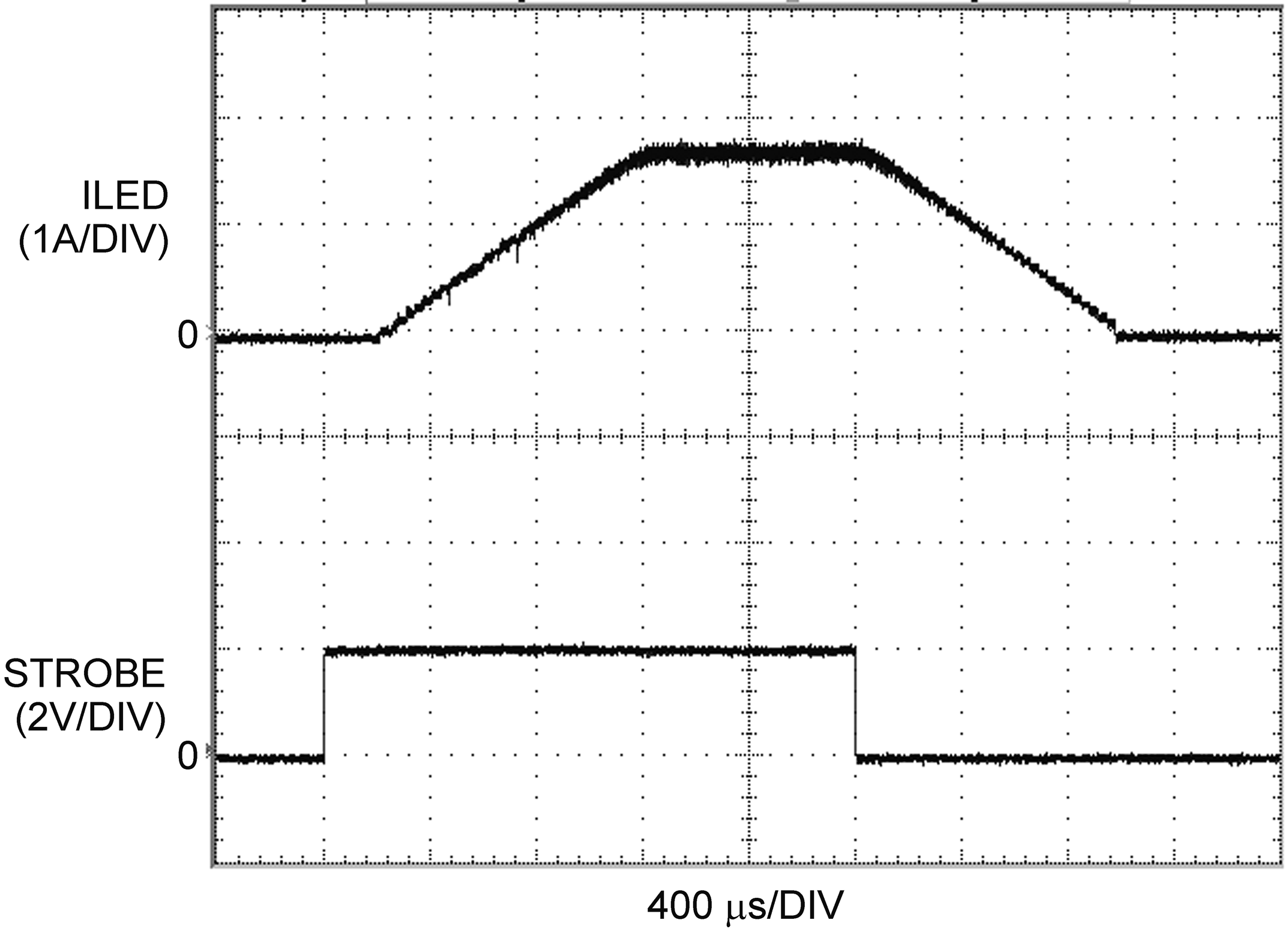
Figure 17. Strobe High-to-Flash LED Current
LM3559 30102883.png
Figure 19. VIN Flash Monitor Operation
LM3559 30102878.png
Figure 21. AET-Mode Operation
LM3559 30102880.png
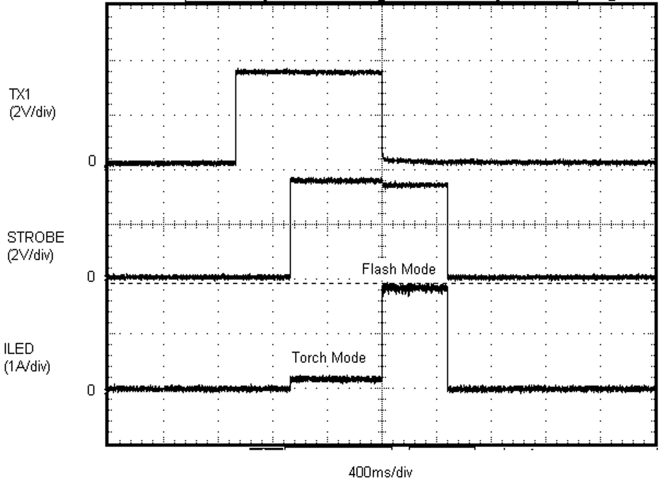
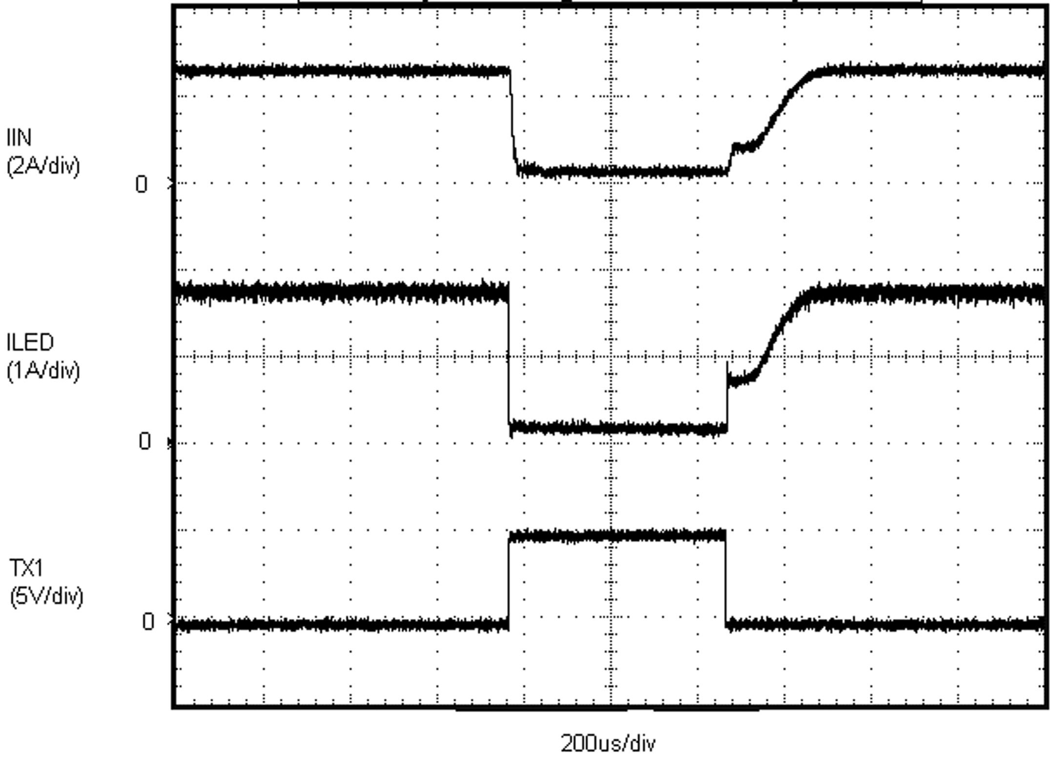
Figure 23. TX1 Interrupt (Force Torch)
LM3559 30102886.png
Register Bits [6:5] = 01
Figure 2. Closed Loop Current Limit vs VIN Flash Duration1
LM3559 30102888.png
Register Bits [6:5] = 11
Figure 4. Closed Loop Current Limit vs VIN Flash Duration1
LM3559 30102898.png
VHWEN= 0 V
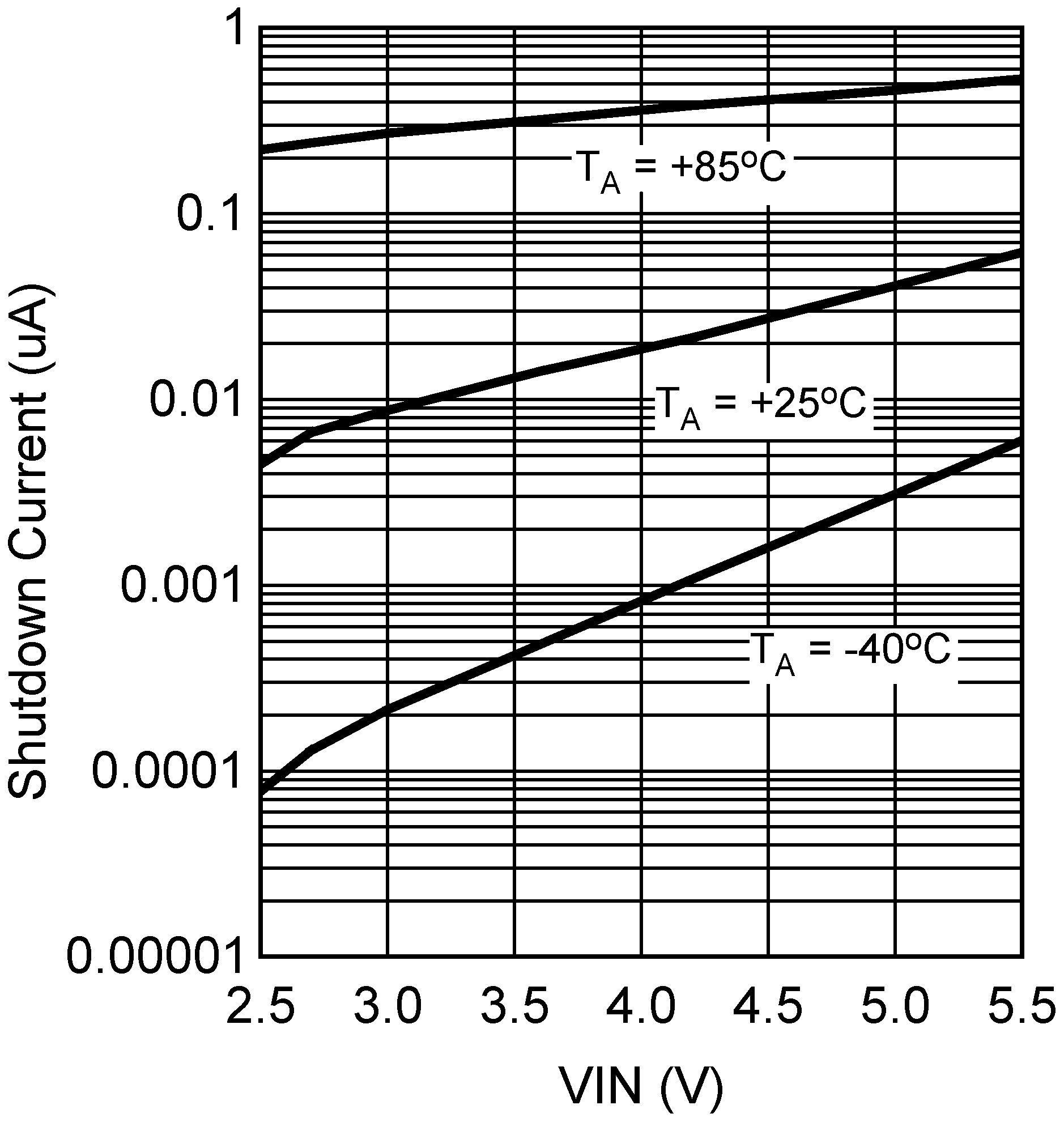
Figure 6. Shutdown Current vs VIN
LM3559 30102862.gif
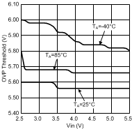
Figure 8. OVP Thresholds vs VIN2
LM3559 30102867.gif
Register Bits [2:0] = 0x00
Figure 10. Indicator Currents vs VIN Indicator
LM3559 30102876.gif
Register Bits [2:0] = 0x07
Figure 12. Indicator Current vs VIN Indicator
LM3559 30102873.gif
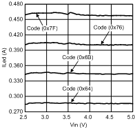
Middle 5 Flash Brightness Codes
Figure 14. ILED (Flash Mode) vs VIN LED1 and LED2 Connected Together
LM3559 30102875.gif
Lower 4 Torch Brightness Codes
Figure 16. ILED (Torch Mode) vs VIN LED1 and LED2 Connected Together
LM3559 30102882.png
Figure 18. VIN Monitor Operation
LM3559 30102884.png
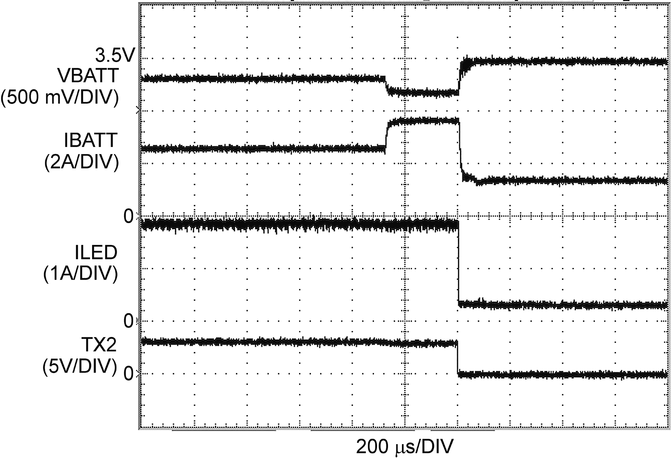
Figure 20. NTC-Mode Operation
LM3559 30102879.png
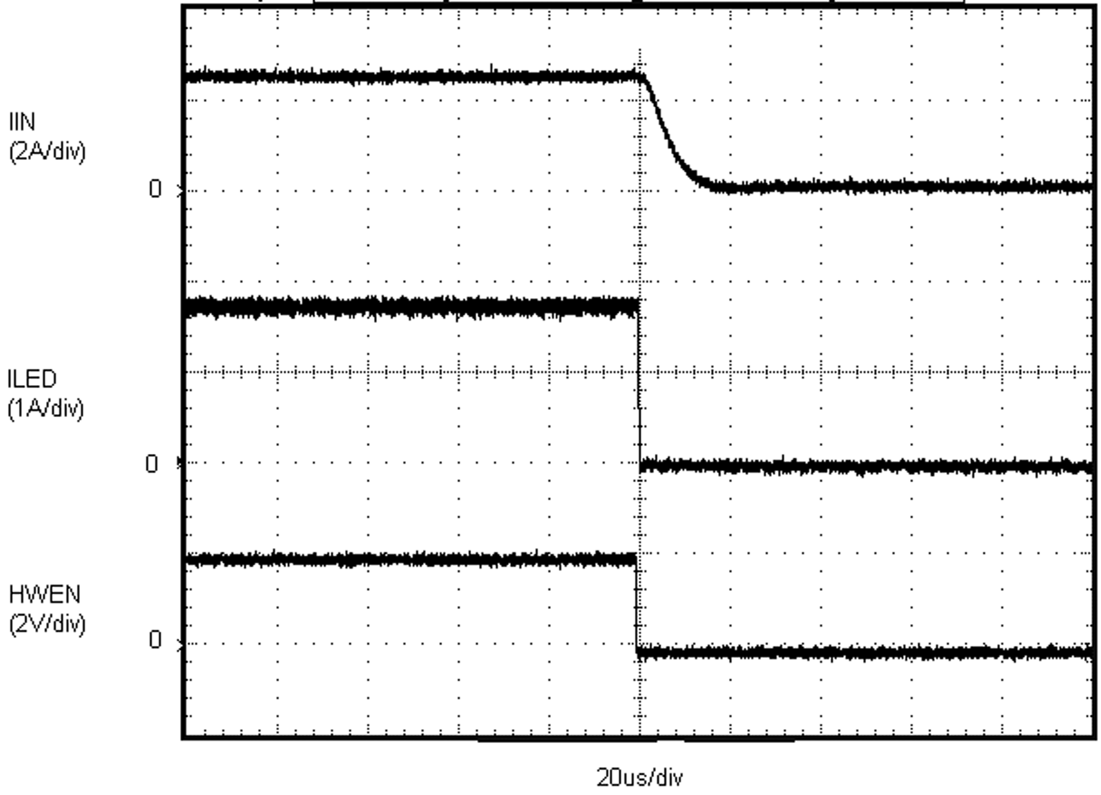
Figure 22. HWEN Operation Device Enabled in Flash Mode
LM3559 30102881.png
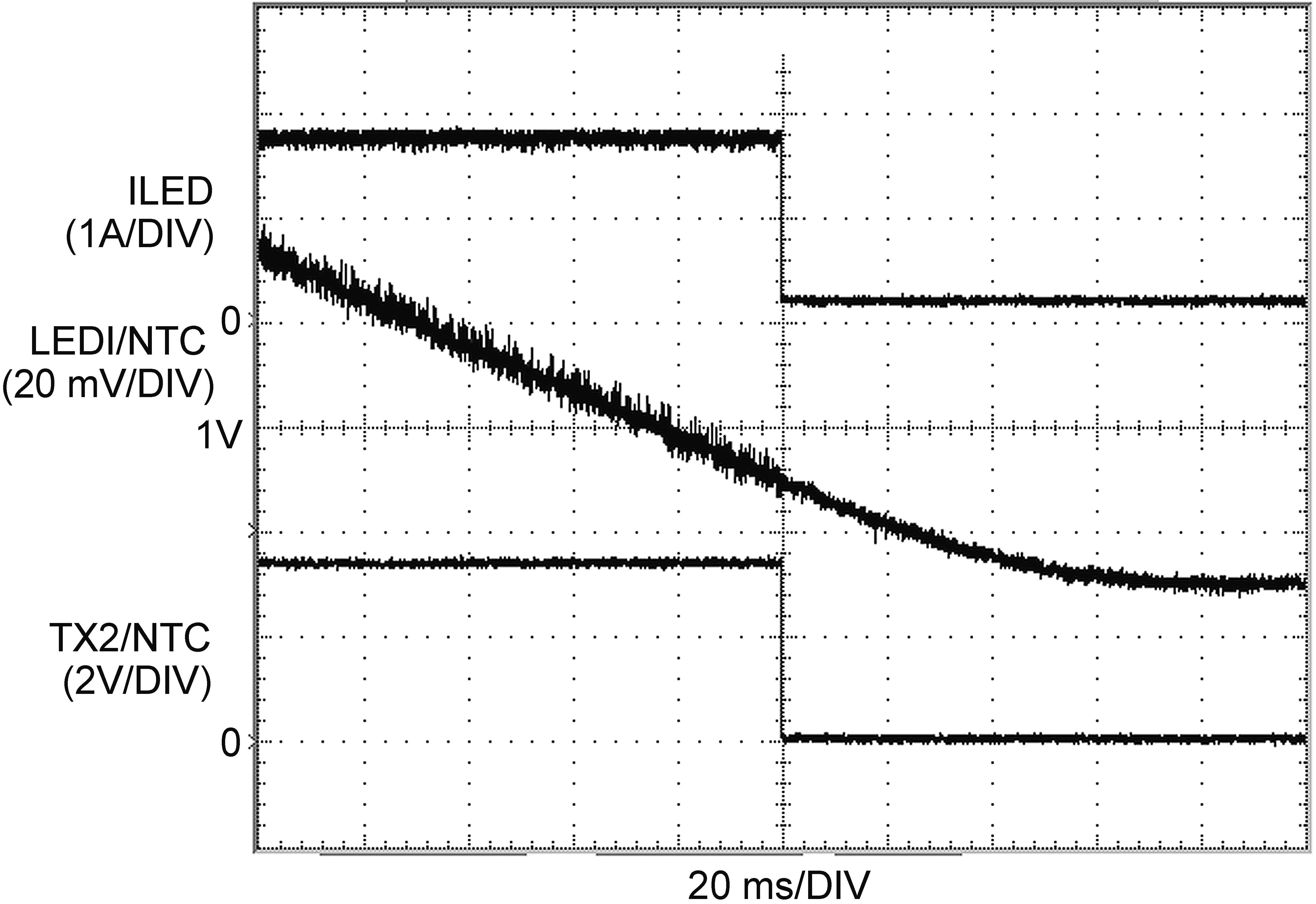
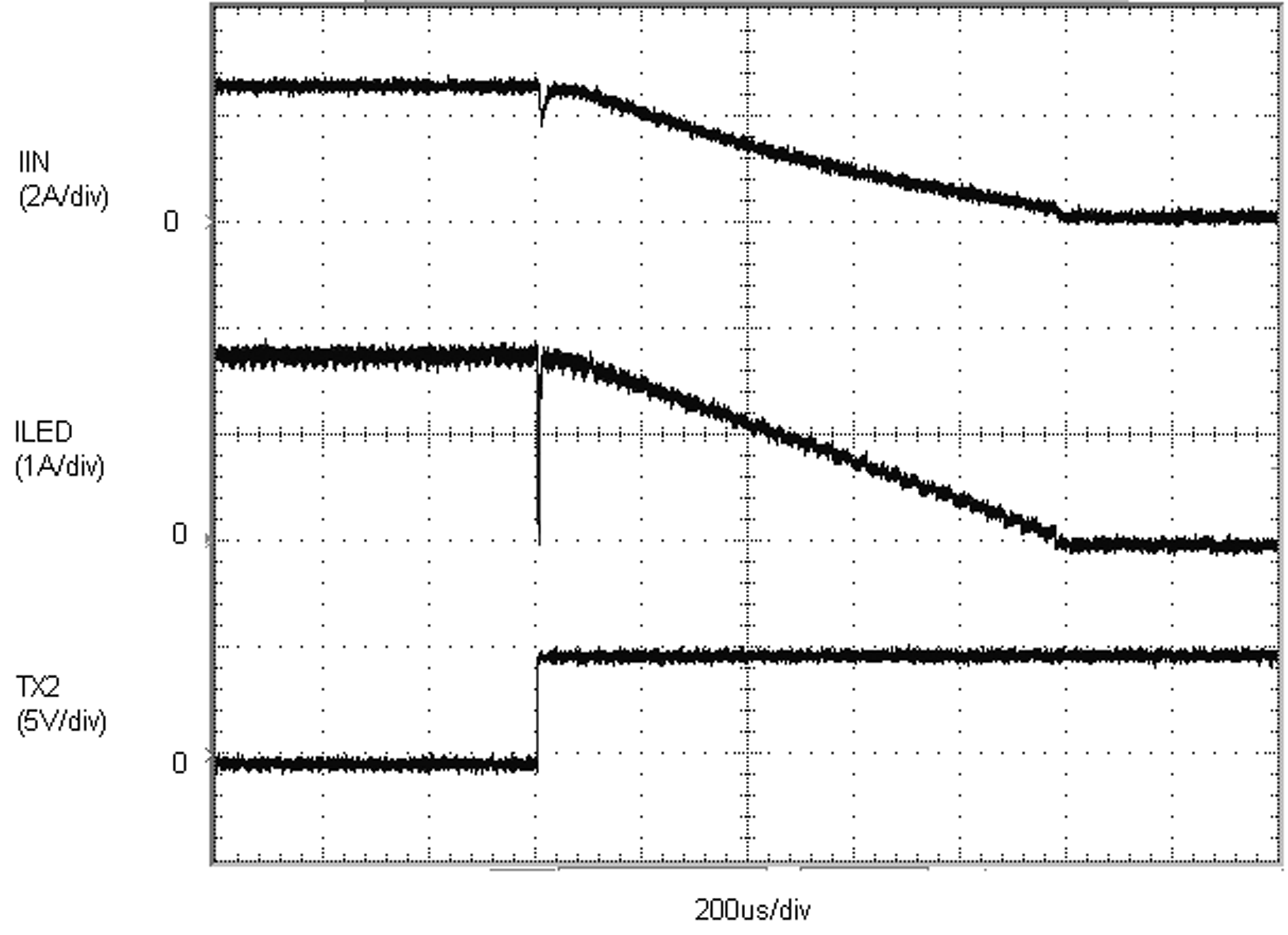
TX2 Active High
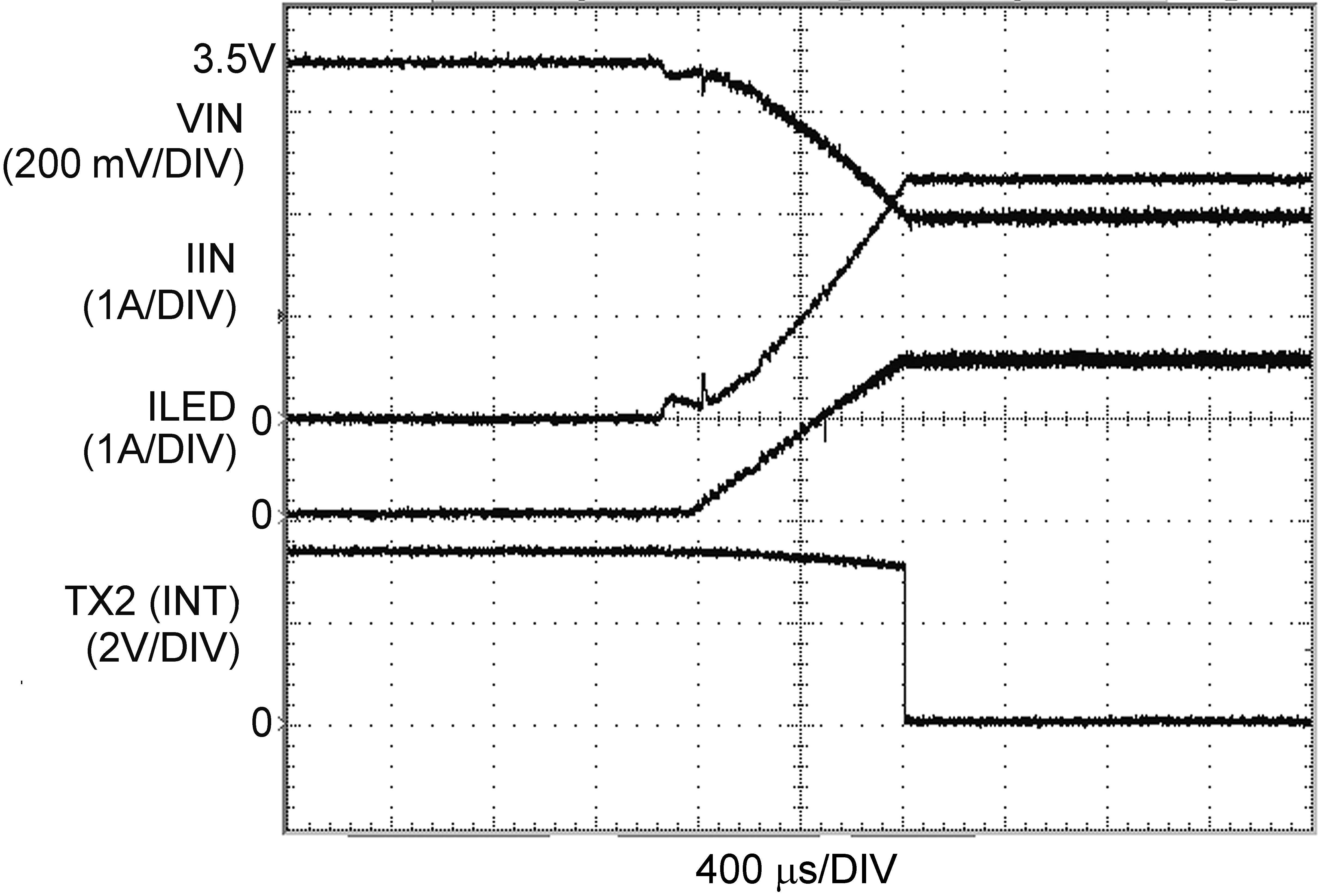
Figure 24. TX2 Interrupt (Forced Shutdown)
1. The typical curve for current limit is measured in closed loop using Figure 43, and increasing IOUT until the peak inductor current stops increasing. The value given in Electrical Characteristics is measured open loop and is found by forcing current into SW until the current limit comparator threshold is reached. Closed loop data appears higher due to the delay between the comparator trip point and the NFET turning off. This delay allows the closed loop inductor current to ramp higher after the trip point by approximately 20 ns × VIN/L.
2. The typical curve for overvoltage protection (OVP) is measured in closed loop using Figure 43 . The OVP value is found by forcing an open circuit in the LED1 and LED2 path and recording the peak value of VOUT. The value given in Electrical Characteristics is found in an open loop configuration by ramping the voltage at OUT until the OVP comparator trips. The closed loop data can appear higher due to the stored energy in the inductor being dumped into the output capacitor after the OVP comparator trips. Worst case is an open circuit condition where the output voltage can continue to rise after the OVP comparator trips by approximately IIN × sqrt(L/COUT).