SNVSA63A April 2015 – September 2015 LM3632A
PRODUCTION DATA.
- 1 Features
- 2 Applications
- 3 Description
- 4 Revision History
- 5 Pin Configuration and Functions
- 6 Specifications
-
7 Detailed Description
- 7.1 Overview
- 7.2 Functional Block Diagram
- 7.3
Features Description
- 7.3.1 Backlight
- 7.3.2 LCM Bias
- 7.3.3 Flash
- 7.3.4 Software RESET
- 7.3.5 EN Input
- 7.3.6 Thermal Shutdown (TSD)
- 7.4 Device Functional Modes
- 7.5 Programming
- 7.6
Register Maps
- 7.6.1 Revision (Address = 0x01) [reset = 0x09]
- 7.6.2 Backlight Configuration1 (Address = 0x02) [reset = 0x30]
- 7.6.3 Backlight Configuration2 (Address = 0x03) [reset = 0x0D]
- 7.6.4 Backlight Brightness LSB (Address = 0x04) [reset = 0x07]
- 7.6.5 Backlight Brightness MSB (Address = 0x05) [reset = 0xFF]
- 7.6.6 Flash/Torch Current (Address = 0x06) [reset = 0x3E]
- 7.6.7 Flash Configuration (Address = 0x07) [reset = 0x2F]
- 7.6.8 VIN Monitor (Address = 0x08) [reset = 0x03]
- 7.6.9 I/O Control (Address = 0x09) [reset = 0x00]
- 7.6.10 Enable (Address = 0x0A) [reset = 0x00]
- 7.6.11 Flags1 (Address = 0x0B) [reset = 0x00]
- 7.6.12 Display Bias Configuration (Address = 0x0C) [reset = 0x18]
- 7.6.13 LCM Boost Bias (Address = 0x0D) [reset = 0x1E]
- 7.6.14 VPOS Bias (Address = 0x0E) [reset = 0x1E]
- 7.6.15 VNEG Bias (Address = 0x0F) [reset = 0x1C]
- 7.6.16 Flags2 (Address = 0x10) [reset = 0x00]
- 8 Application and Implementation
- 9 Power Supply Recommendations
- 10Layout
- 11Device and Documentation Support
- 12Mechanical, Packaging, and Orderable Information
Package Options
Mechanical Data (Package|Pins)
- YFF|30
Thermal pad, mechanical data (Package|Pins)
Orderable Information
6 Specifications
6.1 Absolute Maximum Ratings(1)
Over operating free-air temperature range (unless otherwise noted)| MIN | MAX | UNIT | ||
|---|---|---|---|---|
| Voltage on VIN, FL_SW, FL_OUT, FLED, EN, LCM_EN1, LCM_EN2, PWM, STROBE, TX, SCL, SDA | –0.3 | 6 | V | |
| Voltage on LCM_SW, LCM_OUT, VPOS, C1 | –0.3 | 7 | V | |
| Voltage on VNEG, C2 | –7 | 0.3 | V | |
| Voltage on BL_SW, BL_VOUT, BLED1, BLED2 | –0.3 | 30 | V | |
| Continuous power dissipation | Internally limited | |||
| Maximum junction temperature, TJ(MAX) | 150 | °C | ||
| Storage temperature, Tstg | –45 | 150 | ||
(1) Stresses beyond those listed under Absolute Maximum Ratings may cause permanent damage to the device. These are stress ratings only, which do not imply functional operation of the device at these or any other conditions beyond those indicated under Recommended Operating Conditions. Exposure to absolute-maximum-rated conditions for extended periods may affect device reliability.
6.2 ESD Ratings
| VALUE | UNIT | |||
|---|---|---|---|---|
| V(ESD) | Electrostatic discharge | Human-body model (HBM), per ANSI/ESDA/JEDEC JS-001(1) | ±2000 | V |
| Charged-device model (CDM), per JEDEC specification JESD22-C101(2) | ±1000 | |||
(1) JEDEC document JEP155 states that 500-V HBM allows safe manufacturing with a standard ESD control process.
(2) JEDEC document JEP157 states that 250-V CDM allows safe manufacturing with a standard ESD control process.
6.3 Recommended Operating Conditions
Over operating free-air temperature range (unless otherwise noted).| MIN | MAX | UNIT | ||
|---|---|---|---|---|
| Input voltage, VIN | 2.7 | 5 | V | |
| Operating ambient temperature, TA (1) | –40 | 85 | °C | |
(1) In applications where high power dissipation and/or poor package thermal resistance is present, the maximum ambient temperature may have to be derated. Maximum ambient temperature (TA-MAX) is dependent on the maximum operating junction temperature (TJ-MAX-OP = 125ºC), the maximum power dissipation of the device in the application (PD-MAX), and the junction-to-ambient thermal resistance of the part/package in the application (RθJA), as given by the following equation: TA-MAX = TJ-MAX-OP – (RθJA × PD-MAX).
6.4 Thermal Information
| THERMAL METRIC(1) | LM3632A | UNIT | |
|---|---|---|---|
| YFF (DSBGA) | |||
| 30 PINS | |||
| RθJA | Junction-to-ambient thermal resistance | 58.6 | °C/W |
| RθJC | Junction-to-case (top) thermal resistance | 0.2 | |
| RθJB | Junction-to-board thermal resistance | 8.3 | |
| ΨJT | Junction-to-top characterization parameter | 1.4 | |
| ΨJB | Junction-to-board characterization parameter | 8.3 | |
(1) For more information about traditional and new thermal metrics, see the Semiconductor and IC Package Thermal Metrics application report, SPRA953.
6.5 Electrical Characteristics
Unless otherwise specified, limits apply over the full operating ambient temperature range (−40°C ≤ TA ≤ 85°C), VIN = 3.7 V, VVPOS = 5.5 V, VVNEG = –5.4 V, VLCM_OUT = 6 V.| PARAMETER | TEST CONDITION | MIN | TYP | MAX | UNIT | ||
|---|---|---|---|---|---|---|---|
| CURRENT CONSUMPTION | |||||||
| ISD | Shutdown current | EN = 0 | 1 | 4 | µA | ||
| IQ | Quiescent current, device not switching | EN = VIN, LCD bias boost disabled | 2 | 10 | µA | ||
| ILCD_EN | LCD bias boost enabled, no-load | 0.5 | mA | ||||
| DEVICE PROTECTION | |||||||
| TSD | Thermal shutdown | 140 | °C | ||||
| BACKLIGHT LED CURRENT SINKS | |||||||
| ILED_MAX | Maximum output current in BLED1/2 | 2.7 V ≤ VIN ≤ 5 V, linear or exponential mode | 25 | mA | |||
| ILED_MIN | Minimum output current in BLED1/2 | 2.7 V ≤ VIN ≤ 5 V, linear or exponential mode | 50 | µA | |||
| IACCU | LED current accuracy(1) | 2.7 V ≤ VIN ≤ 5 V, 50 µA ≤ ILED ≤ 25 mA, linear or exponential mode | -3% | 0.1% | 3% | ||
| IMATCH | LED1 to LED2 current matching(1) | 2.7 V ≤ VIN ≤ 5 V, 300 µA ≤ ILED ≤ 25 mA, linear or exponential mode | -2% | 0.1% | 2% | ||
| BACKLIGHT BOOST CONVERTER | |||||||
| VOVP_BL | Backlight boost output overvoltage protection | 2.7 V ≤ VIN ≤ 5 V, 29 V option | 28 | 28.75 | 29.5 | V | |
| Efficiency | Typical efficiency(2) | ILED = 5 mA/string, VIN = 3.7 V (2 x 7 LEDs), (POUT/PIN) |
87% | ||||
| VHR | Regulated current sink headroom voltage | ILED = 25 mA | 250 | mV | |||
| ILED = 5 mA | 100 | mV | |||||
| VHR_MIN | Current sink minimum headroom voltage | ILED = 95% of nominal, ILED = 5 mA | 30 | mV | |||
| RDSON | NMOS switch on resistance | ISW = 100 mA | 0.25 | Ω | |||
| ICL | NMOS switch current limit | 2.7 V ≤ VIN ≤ 5 V | 900 | 1000 | 1100 | mA | |
| ƒSW_BLBOOST | Switching frequency | 2.7 V ≤ VIN ≤ 5 V | 500-kHz mode | 450 | 500 | 550 | kHz |
| 1-MHz mode | 900 | 1000 | 1100 | ||||
| DMAX | Maximum duty cycle | 94% | |||||
| LCM BIAS BOOST CONVERTER | |||||||
| VOVP_LCM | LCM bias boost output overvoltage protection | 2.7 V ≤ VIN ≤ 5 V | 7 | V | |||
| ƒSW_LCMBST | Switching frequency (3) | 2.7 V ≤ VIN ≤ 5 V | 2500 | kHz | |||
| VLCM_OUT | Bias boost output voltage range | 4.5 | 6.4 | V | |||
| Output voltage step size | 50 | mV | |||||
| Peak-to-peak ripple voltage (3) | ILOAD = 5 mA & 50 mA, CBST = 10 µF | 50 | mVpp | ||||
| LCM_OUT line transient response (3) | VIN + 500 mVp-p AC square wave, Tr = 100 mV/µs, 200 Hz, 12.5 % duty, ILOAD = 5 mA, CIN = 10 µF | –50 | ±25 | 50 | mV | ||
| LCM_OUT load transient response (3) | Load current step 0 mA to 100 mA, TRISE/FALL = 100 mA/µs, CIN = 10 µF | –150 | 150 | mV | |||
| ICL_LCMBST | Valley current limit | 1000 | mA | ||||
| RDSON_LCMBST | High-side MOSFET on resistance | VIN = VGS = 5 V, TA = 25°C | 170 | mΩ | |||
| Low-side MOSFET on Resistance | VIN = VGS = 5 V, TA = 25°C | 290 | |||||
| EFFLCMBST | Efficiency (2) | VLCM_OUT = 6 V, 5 mA < ILCMBST < 100 mA | 92% | ||||
| tST_LCMBST | Start-up time (LCM_OUT), VLCM_OUT = 10% to 90% (3) | CLCM_BST = 10 µF | 1000 | µs | |||
| DISPLAY BIAS POSITIVE OUTPUT (VPOS) | |||||||
| VVPOS | Programmable output voltage range | 4 | 6 | V | |||
| Output voltage step size | 50 | mV | |||||
| Output voltage accuracy | Output voltage = 5.4 V | –1.5% | 1.5% | ||||
| VPOS line transient response (3) | VIN + 500 mVp-p AC square wave, Tr = 100 mV/µs, 200 Hz, ILOAD = 25 mA, CIN = 10 µF | –50 | 50 | mV | |||
| VPOS load transient response (3) | 0 to 50 mA load transient, CVPOS = 10 µF | –50 | 50 | mV | |||
| DC load regulation (3) | 0 mA ≤ IVPOS ≤ 50 mA | 20 | mV | ||||
| IMAX_VPOS | Maximum output current | 50 | mA | ||||
| ICL_VPOS | Output current limit | 80 | mA | ||||
| IRUSH_PK_VPOS | Peak start-up inrush current (3) | VLCM_OUT = 6.3 V, VPOS = 5.8 V, CVPOS = 10 µF | 250 | mA | |||
| VDO_VPOS | VPOS dropout voltage (4) | IVPOS = 50 mA, VVPOS = 5.5 V | 100 | mV | |||
| tST_VPOS | Start-up time VPOS, VVPOS = 10% to 90% (3) | CVPOS = 10 µF | 500-µs setting | 500 | µs | ||
| 800-µs setting | 800 | ||||||
| RPD_VPOS | Output pull-down resistor (VPOS) | VPOS disabled | 30 | 80 | 110 | Ω | |
| DISPLAY BIAS NEGATIVE OUTPUT (VNEG) | |||||||
| VOVP_VNEG | LCM bias negative charge-pump output overvoltage protection | Below VVNEG output voltage target | –250 | mV | |||
| VSHORT_VNEG | LCM bias negative charge-pump output short circuit protection | VNEG to CP_GND | –750 | mV | |||
| VVNEG | Programmable output voltage range | –6 | –4 | V | |||
| Output voltage step size | 50 | mV | |||||
| Output accuracy | Output voltage = –5.4 V | –1.5% | 1.5% | ||||
| Peak-to-peak ripple voltage(3) | ILOAD = 5 mA & 50 mA, CVNEG = 10 µF |
60 | mVpp | ||||
| VNEG line transient response(3) | VIN + 500 mVp-p AC square wave, 100 mV/µs 200 Hz, 12.5% duty at 5 mA | –50 | ±25 | 50 | mV | ||
| VNEG load transient response(3) | 0 to 50 mA load transient, TRISE/FALL = 1 µs, CVNEG = 10 µF |
100 | mV | ||||
| Efficiency(2) | VIN = 3.7 V, VLCM_OUT = 5.8 V, VVNEG = –5.4 V, IVNEG > 5 mA |
92% | |||||
| IMAX_VNEG | Maximum output current(3) | VIN = 3.7 V, VLCM_OUT = 5.8 V, VVNEG = –5.4 V |
50 | mA | |||
| ICL_VNEG | Output current limit(3) | 75 | mA | ||||
| RDSON_VNEG | Charge FET pump on resistance | Q1 | 350 | mΩ | |||
| Q2 | 400 | ||||||
| Q3 | 400 | ||||||
| tST_VNEG | Start-up time (VVNEG), VVNEG = 10% to 90%(3) | VVNEG = –6 V, CVNEG = 10 µF | 1 | ms | |||
| RPU_VNEG | Output pullup resistor, VNEG(3) | VNEG Disabled, VLCM_OUT > 4.8 V | 20 | 40 | Ω | ||
| FLASH DRIVER BOOST | |||||||
| ILED | Current source accuracy | 1.5-A flash, VFL_OUT = 4 V | 1.4 | 1.5 | 1.6 | A | |
| VOVP | Output overvoltage protection trip point | ON threshold | 4.85 | 5 | 5.1 | V | |
| OFF threshold | 4.75 | 4.9 | 5 | ||||
| VHR | Current source regulation voltage | 1.5-A flash, VFL_OUT = 4 V | 275 | mV | |||
| ICL | Switch current limit | 2.45 | 2.8 | 3.15 | A | ||
| 1.65 | 1.9 | 2.15 | |||||
| RNMOS | NMOS switch on resistance | INMOS = 1 A | 80 | mΩ | |||
| RPMOS | PMOS switch on resistance | IPMOS = 1 A | 100 | ||||
| VVINM | Input voltage monitor trip threshold | 2.76 | 2.9 | 3.04 | V | ||
| LOGIC INPUTS (PWM, EN, LCM_EN1, LCM_EN2, SCL, SDA, TX, STROBE) | |||||||
| VIL | Input logic low | 0 | 0.4 | V | |||
| VIH | Input logic high | 1.2 | VIN | V | |||
| LOGIC OUTPUTS (SDA) | |||||||
| VOL | Output logic low | 2.7 V ≤ VIN ≤ 5 V, IOL = 3 mA | 0 | 0.4 | V | ||
| PWM INPUT | |||||||
| ƒPWM_INPUT | PWM input frequency(2) | 100 | 20000 | Hz | |||
| Minimum PWM ON/OFF time(3) | PWM sampling frequency = 1 MHz | 6 | µs | ||||
| PWM sampling frequency = 4 MHz | 1.5 | ||||||
| PWM timeout(3) | PWM sampling frequency = 1 MHz | 25 | ms | ||||
| PWM sampling frequency = 4 MHz | 3 | ||||||
(1) Output Current Accuracy is the difference between the actual value of the output current and programmed value of this current. Matching is the maximum difference from the average. For the constant current sinks on the device (BLED1 and BLED2), the following is determined: the maximum output current (MAX), the minimum output current (MIN), and the average output current of both outputs (AVG). Matching number is calculated: (ILED1 – ILED2)/(ILED1 + ILED2). The typical specification provided is the most likely norm of the matching figure of all parts. Note that some manufacturers have different definitions in use.
(2) Typical value only for information.
(3) Limits set by characterization and/or simulation only.
(4) VIN_VPOS – VVPOS when VVPOS has dropped 100 mV below target.
6.6 I2C Timing Requirements (SDA, SCL) (1)
Over operating free-air temperature range (unless otherwise noted)(see Figure 1).| MIN | NOM | MAX | UNIT | ||
|---|---|---|---|---|---|
| ƒSCL | Clock frequency | 400 | kHz | ||
| 1 | Hold time (repeated) START condition | 0.6 | µs | ||
| 2 | Clock low time | 1.3 | µs | ||
| 3 | Clock high time | 600 | ns | ||
| 4 | Set-up time for a repeated START condition | 600 | ns | ||
| 5 | Data hold time | 50 | ns | ||
| 6 | Data set-up time | 100 | ns | ||
| 7 | Rise time of SDA and SCL | 20 + 0.1Cb | 300 | ns | |
| 8 | Fall time of SDA and SCL | 15 + 0.1Cb | 300 | ns | |
| 9 | Set-Up time between a STOP and a START condition | 1.3 | µs | ||
| Cb | Capacitive load for each bus line | 10 | 200 | pF | |
(1) Limits set by characterization and/or simulation only.
 Figure 1. I2C Timing Parameters
6.7 Typical Characteristics
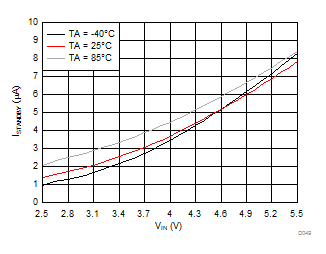
Ambient temperature is 25°C and VIN is 3.7 V unless otherwise noted.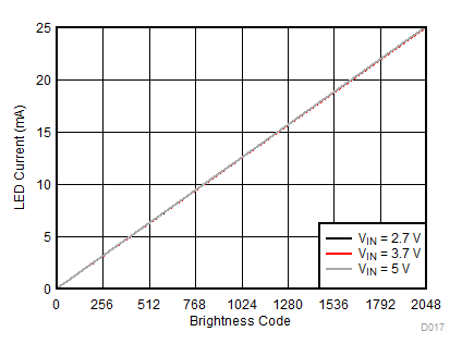
| 2p6s LEDs | ||
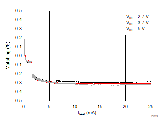
| 2p6s LEDs | ||
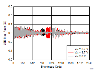
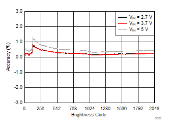
| 2p6s LEDs | ||
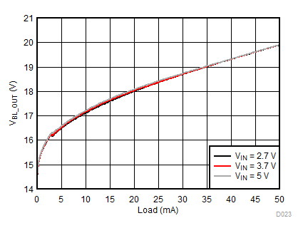
| 2p6s LEDs | ||
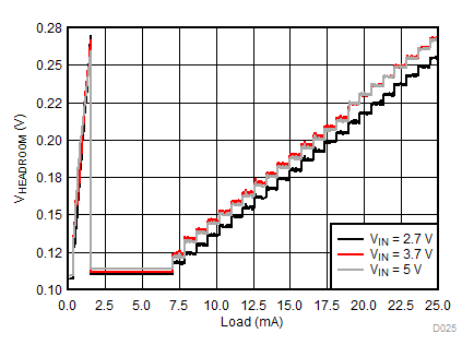
| 2p6s LEDs | ||
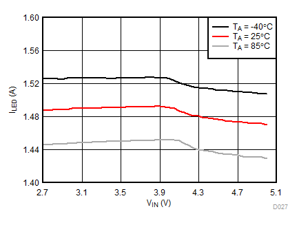
| IFLED = 1.5 A | ƒ = 4 MHz | |
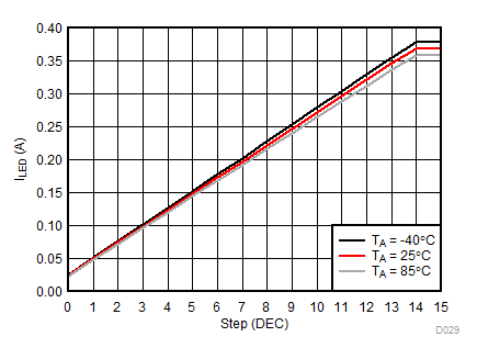
| ƒ = 4MHz | ||
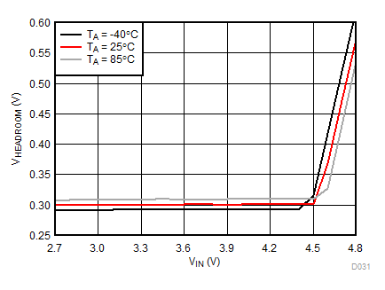
| IFLED = 1.5 A | ƒ = 4 MHz | VFLED = 4 V |
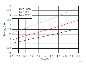
| VEN = VIN | I2C = VIN | |
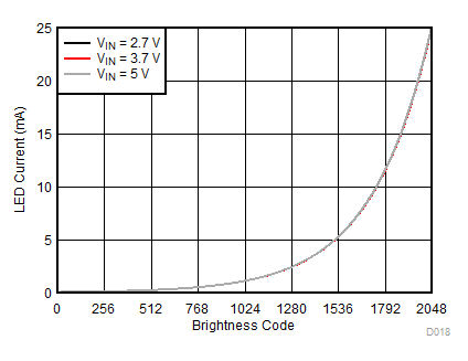
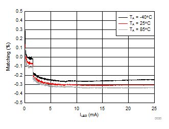
| 2p6s LEDs | ||
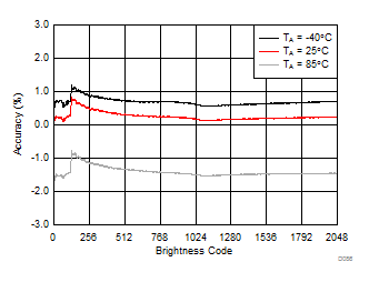
| 2p6s LEDs | ||
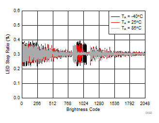
| 2p6s LEDs | ||
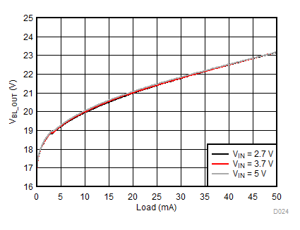
| 2p7s LEDs | ||
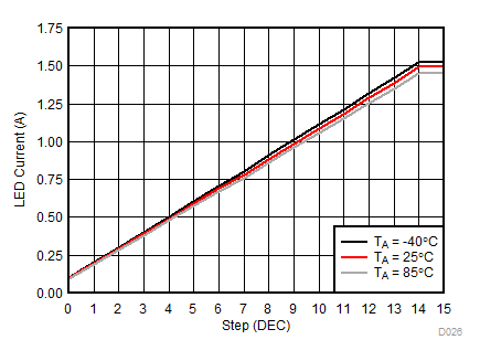
| ƒ = 4 MHz | ||
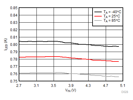
| IFLED = 0.8 A | f = 4 MHz | |
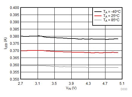
| IFLED = 375 mA | ƒ = 4 MHz | |
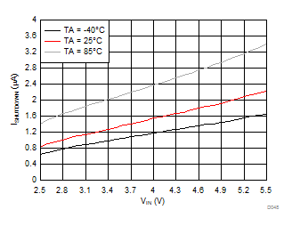
| VEN = 0 V | I2C = 0 V | |
