SNVS867 June 2014 LM3633
PRODUCTION DATA.
- 1 Features
- 2 Applications
- 3 Description
- 4 Revision History
- 5 Pin Configuration and Functions
- 6 Specifications
-
7 Detailed Description
- 7.1 Overview
- 7.2 Functional Block Diagram
- 7.3 Feature Description
- 7.4
Device Functional Modes
- 7.4.1
High-Voltage LED Control
- 7.4.1.1 High-Voltage Boost Converter
- 7.4.1.2 High-Voltage Current Sinks (HVLED1, HVLED2 and HVLED3)
- 7.4.1.3 High-Voltage Current String Biasing
- 7.4.1.4 Boost Switching-Frequency Select
- 7.4.1.5 Automatic Switching Frequency Shift
- 7.4.1.6 Brightness Register Current Control
- 7.4.1.7 PWM Control
- 7.4.1.8 Start-up/Shutdown Ramp
- 7.4.1.9 Run-Time Ramp
- 7.4.1.10 High-Voltage Control A/B Ramp Select
- 7.4.1.11 LED Current Mapping Modes
- 7.4.1.12 Exponential Mapping
- 7.4.1.13 Linear Mapping
- 7.4.2
Low-Voltage LED Control
- 7.4.2.1 Integrated Charge Pump
- 7.4.2.2 Charge Pump Disabled
- 7.4.2.3 Automatic Gain
- 7.4.2.4 Automatic Gain (Flying Capacitor Detection)
- 7.4.2.5 1X Gain
- 7.4.2.6 2X Gain
- 7.4.2.7 Low-Voltage Current Sinks (LVLED1 to LVLED6)
- 7.4.2.8 Low-Voltage LED Biasing
- 7.4.2.9 Brightness Register Current Control
- 7.4.2.10 LED Current Mapping Modes
- 7.4.2.11 Exponential Mapping
- 7.4.2.12 Linear Mapping
- 7.4.2.13 Start-up/Shutdown Ramp
- 7.4.2.14 Run-Time Ramp
- 7.4.3 Low-Voltage LED Pattern Generator
- 7.4.4 Fault Flags/Protection Features
- 7.4.5 I2C-Compatible Interface
- 7.4.1
High-Voltage LED Control
- 7.5 Register Descriptions
-
8 Applications and Implementation
- 8.1 Application Information
- 8.2
Typical Application
- 8.2.1 Design Requirements
- 8.2.2
Detailed Design Procedure
- 8.2.2.1 Boost Converter Maximum Output Power (Boost)
- 8.2.2.2 Boost Inductor Selection
- 8.2.2.3 Output Capacitor Selection
- 8.2.2.4 Schottky Diode Selection
- 8.2.2.5 Input Capacitor Selection
- 8.2.2.6 Maximum Output Power (Charge Pump)
- 8.2.2.7 Charge Pump Flying Capacitor Selection
- 8.2.2.8 Charge Pump Output Capacitor Selection
- 8.2.2.9 Charge Pump Input Capacitor Selection
- 8.2.3 Application Performance Plots
- 8.3 Initialization Set Up
- 9 Power Supply Recommendations
- 10Layout
- 11Device and Documentation Support
- 12Mechanical, Packaging, and Orderable Information
Package Options
Mechanical Data (Package|Pins)
- YFQ|20
Thermal pad, mechanical data (Package|Pins)
Orderable Information
6 Specifications
6.1 Absolute Maximum Ratings
over operating free-air temperature range (unless otherwise noted)(1)| MIN | MAX | UNIT | ||
|---|---|---|---|---|
| VIN to GND | −0.3 | 6 | V | |
| VSW, VOVP, VHVLED1, VHVLED2, VHVLED3 to GND | −0.3 | 45 | ||
| VSCL, VSDA, VPWM to GND | −0.3 | 6 | ||
| VHWEN, VCPOUT to GND, VC–, VC+ | −0.3 | 6 | ||
| VLVLED1- VLVLED6, to GND | −0.3 | 6 | ||
| Continuous power dissipation | Internally Limited | |||
| Junction temperature (TJ-MAX) | 150 | °C | ||
(1) Stresses beyond those listed under absolute maximum ratings may cause permanent damage to the device. These are stress ratings only, which do not imply functional operation of the device at these or any other conditions beyond those indicated under recommended operating conditions. Exposure to absolute–maximum–rated conditions for extended periods may affect device reliability.
6.2 Handling Ratings
| MIN | MAX | UNIT | |||
|---|---|---|---|---|---|
| Tstg | Storage temperature range | −65 | 150 | °C | |
| V(ESD) | Electrostatic discharge | Human body model (HBM), per ANSI/ESDA/JEDEC JS-001, all pins(1) | −1000 | 1000 | V |
| Charged device model (CDM), per JEDEC specification JESD22-C101, all pins(2) | −250 | 250 | |||
(1) JEDEC document JEP155 states that 500-V HBM allows safe manufacturing with a standard ESD control process.
(2) JEDEC document JEP157 states that 250-V CDM allows safe manufacturing with a standard ESD control process.
6.3 Recommended Operating Conditions
over operating free-air temperature range (unless otherwise noted)| MIN | NOM | MAX | UNIT | ||
|---|---|---|---|---|---|
| VIN to GND | 2.7 | 5.5 | V | ||
| VSW, VOVP, VHVLED1, VVHLED2, VVHLED3 to GND, VPWM, VHWEN, VSDA, VSCL | 0 | 40 | |||
| VLVLED1- VLVLED6 to GND | 0 | 6 | |||
| Junction temperature (TJ) (1)(2) | −40 | 125 | °C | ||
(1) Internal thermal shutdown circuitry protects the device from permanent damage. Thermal shutdown engages at TJ = 140°C (typ.) and disengages at TJ= 125°C (typ.).
(2) In applications where high power dissipation and/or poor package thermal resistance is present, the maximum ambient temperature may have to be derated. Maximum ambient temperature (TA-MAX) is dependent on the maximum operating junction temperature (TJ-MAX-OP = 125°C), the maximum power dissipation of the device in the application (PD-MAX), and the junction-to ambient thermal resistance of the part/package in the application (θJA), as given by the following equation: TA-MAX = TJ-MAX-OP – (θJA × PD-MAX).
6.4 Thermal Information
| THERMAL METRIC(1) | DSBGA | UNIT | |
|---|---|---|---|
| (20 PINS) | |||
| RθJA | Thermal resistance junction-to-ambient | 55.3 | °C/W |
(1) For more information about traditional and new thermal metrics, see the IC Package Thermal Metrics application report, SPRA953.
6.5 Electrical Characteristics
Limits apply over the full operating ambient temperature range (−40°C ≤ TA ≤ 85°C) and VIN = 3.6 V, unless otherwise specified.(1)(2)| PARAMETER | TEST CONDITIONS | MIN | TYP | MAX | UNIT | ||
|---|---|---|---|---|---|---|---|
| SUPPLY VOLTAGE (IN PIN) | |||||||
| ISHDN | Shutdown current | 2.7 V ≤ VIN ≤ 5.5 V, HWEN = GND | 1 | 5.5 | µA | ||
| THERMAL SHUTDOWN | |||||||
| TSD | Thermal shutdown | 140 | °C | ||||
| Hysteresis | 15 | ||||||
| BOOST CONVERTER AND HVLED | |||||||
| IHVLED(1/2/3) | Output current regulation (HVLED1, HVLED2 or HVLED3) | Full-scale current = 20.2 mA, PWM off, brightness code = max, exponential mapping, auto headroom off, HVLED1 Bank A, HVLED2/3 Bank B | 2.7 V ≤ VIN ≤ 5.5 V | 18.38 (–9%) |
20.2 | 22.02 (9%) |
mA |
| Full-scale current = 20.2 mA, PWM off, brightness code = max, exponential mapping, auto headroom off, HVLED1 Bank A, HVLED2/3 Bank B | TA = 25°C | –3.4% | ±2.0% | 3.2% | |||
| TA = 25°C, 3.0 V ≤ VIN ≤ 4.5 V |
–3.6% | 3.4% | |||||
| TA = 25°C | ±2.0% | ||||||
| IMATCH_HV | HVLED1 to HVLED2 or HVLED3 matching (3) | PWM off, exponential mapping, auto headroom off HVLED1,2,3 = Bank A, |
2.7 V ≤ VIN ≤ 5.5 V, ILED = 20.2 mA |
–2.5% | 2.5% | ||
| TA = 25°C, ILED = 20.2 mA |
–2.0% | 1.7% | |||||
| 2.7 V ≤ VIN ≤ 5.5 V ILED = 500 µA |
–8.5% | 8.5% | |||||
| ILED_MIN | Minimum LED current | Full-scale current = 20.2 mA, Exponential Mapping | 6.0 | µA | |||
| VREG_CS | Regulated current sink headroom voltage | Auto headroom off, TA = 25°C | 400 | mV | |||
| VHR_HV | Minimum current sink headroom voltage for HVLED current sinks | ILED = 95% of nominal, full-scale current = 20.2 mA, auto headroom off | 2.7 V ≤ VIN ≤ 5.5 V | 285 | |||
| TA = 25°C | 190 | ||||||
| RDSON | NMOS switch on resistance | ISW = 500 mA, TA = 25°C | 0.3 | Ω | |||
| ICL_BOOST | NMOS switch current limit | 880 | 1120 | mA | |||
| TA = 25°C | 1000 | ||||||
| VOVP | Output overvoltage protection | ON threshold OVP select bits = 11 |
2.7 V ≤ VIN ≤ 5.5 V | 38.75 | 41.1 | V | |
| TA = 25°C | 40 | ||||||
| Hysteresis | TA = 25°C | 1 | |||||
| fSW | Switching frequency | Boost frequency select bit = 0 | 2.7 V ≤ VIN ≤ 5.5 V | 450 | 550 | kHz | |
| TA = 25°C | 500 | ||||||
| Boost frequency select bit = 1 | 2.7 V ≤ VIN ≤ 5.5 V | 900 | 1100 | ||||
| TA = 25°C | 1000 | ||||||
| DMAX | Maximum duty cycle | 2.7 V ≤ VIN ≤ 5.5 V | 94% | ||||
| CHARGE PUMP AND LVLED | |||||||
| ILVLED(1/2/3/4/5/6) | Output current regulation (low-voltage current sinks) | Full-scale current = 20.2 mA, brightness code = 0xFF | 2.7 V ≤ VIN ≤ 5.5 V | 18.38 | 20.2 | 22.02 | mA |
| IMATCH_LV | LVLED current sink matching (4) | Full-scale current = 20.2 mA | 2.7 V ≤ VIN ≤ 5.5 V | −3.1% | 2% | ||
| VHR_LV | Minimum current sink headroom voltage for LVLED current sinks | ILED = 95% of nominal, full-scale current = 20.2 mA | 125 | mV | |||
| TA = 25°C | 80 | ||||||
| VGTH | Threshold for gain transition | 2.7 V ≤ VIN ≤ 5.5 V | 65 | 190 | |||
| TA = 25°C | 125 | ||||||
| VCPOUT | Charge Pump Output Voltage | 2X Gain | TA = 25°C | 4.42 | V | ||
| ICL_PUMP | Charge pump current limit | 1X Gain, output referred | 3 V ≤ VIN ≤ 5.5 V | 180 | 350 | mA | |
| 2X Gain | TA = 25°C | 240 | |||||
| ROUT | Charge pump output resistance | 1X Gain | TA = 25°C | 1.1 | Ω | ||
| HWEN INPUT | |||||||
| VHWEN_L | Logic low | 2.7 V ≤ VIN ≤ 5.5 V | 0 | 0.4 | V | ||
| VHWEN_H | Logic High | 2.7 V ≤ VIN ≤ 5.5 V | 1.2 | VIN | |||
| PWM INPUT | |||||||
| VPWM_L | Input logic low | 2.7 V ≤ VIN ≤ 5.5 V | 0 | 400 | mV | ||
| VPWM_H | Input logic high | 2.7 V ≤ VIN ≤ 5.5 V | 1.36 | VIN | |||
| tPWM | Minimum PWM input pulse | 2.7 V ≤ VIN ≤ 5.5 V, PWM Zero Detect Enabled | 0.75 | µs | |||
| I2C-COMPATIBLE VOLTAGE SPECIFICATIONS (SCL, SDA) | |||||||
| VIL | Input logic low | 2.7 V ≤ VIN ≤ 5.5 V | 0 | 400 | mV | ||
| VIH | Input logic high | 2.7 V ≤ VIN ≤ 5.5 V | 1.35 | VIN | V | ||
| VOL | Output logic low (SDA) | 2.7 V ≤ VIN ≤ 5.5 V, ILOAD = 3 mA | 400 | mV | |||
(1) All voltages are with respect to the potential at the GND pin.
(2) Minimum and Maximum limits are verified by design, test, or statistical analysis. Typical (Typ) numbers are not verified, but do represent the most likely norm. Unless otherwise specified, conditions for typical specifications are: VIN = 3.6 V and TA = 25°C.
(3) LED current sink matching in the high-voltage current sinks (HVLED1 through HVLED3) is given as the maximum matching value between any two current sinks, where the matching between any two high voltage current sinks (X and Y) is given as (IHVLEDX ( or IHVLEDY) - IAVE(X-Y))/(IAVE(X-Y)) x 100. In this test all three HVLED current sinks are assigned to Bank A.
(4) LED current sink matching in the low-voltage current sinks (LVLED1 through LVLED3 or LVLED4 through LVLED6) is given as the maximum matching value between any two current sinks, where the matching between any two low voltage current sinks (X and Y) is given as (ILVLEDX ( or ILVLEDY) - IAVE(X-Y))/(IAVE(X-Y)) x 100. In this test LVLED1-3 current sinks are assigned to Bank C and LVLED4-6 are assigned to Bank F.
6.6 Timing Requirements
Limits apply over the full operating ambient temperature range (−40°C ≤ TA ≤ 85°C) and VIN = 3.6 V, unless otherwise specified.(1)(2)| PARAMETER | TEST CONDITIONS | MIN | TYP | MAX | UNIT | |
|---|---|---|---|---|---|---|
| I2C-COMPATIBLE TIMING SPECIFICATIONS (SCL, SDA)(3), Figure 1 | ||||||
| t1 | SCL (Clock Period) | 2.7 V ≤ VIN ≤ 5.5 V | 2.5 | µs | ||
| t2 | Data In setup time to SCL high | 2.7 V ≤ VIN ≤ 5.5 V | 100 | ns | ||
| t3 | Data out stable after SCL low | 2.7 V ≤ VIN ≤ 5.5 V | 0 | |||
| t4 | SDA low setup time to SCL low (Start) | 2.7 V ≤ VIN ≤ 5.5 V | 100 | |||
| t5 | SDA high hold time after SCL high (Stop) | 2.7 V ≤ VIN ≤ 5.5 V | 100 | |||
| INTERNAL POR THRESHOLD AND HWEN TIMING SPECIFICATION | ||||||
| VPOR | POR reset release voltage threshold | VIN ramp time = 100 μs | 1.7 | 2.1 | V | |
| VIN ramp time = 100 μs, TA = 25°C | 1.9 | |||||
| tHWEN | First I2C start pulse after HWEN high | POR reset complete, 2.7 V ≤ VIN ≤ 5.5 V | 20 | µs | ||
| POR reset complete, TA = 25°C | 5 | |||||
(1) All voltages are with respect to the potential at the GND pin.
(2) Minimum and Maximum limits are verified by design, test, or statistical analysis. Typical (Typ) numbers are not verified, but do represent the most likely norm. Unless otherwise specified, conditions for typical specifications are: VIN = 3.6 V and TA = 25°C.
(3) SCL and SDA must be glitch-free in order for proper brightness control to be realized.
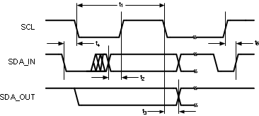 Figure 1. I2C-Compatible Interface Timing
6.7 Typical Characteristics
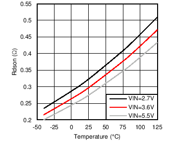 Figure 2. NMOS RDSON vs Temperature
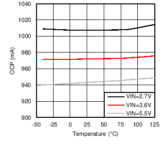 Figure 4. Boost OCP vs Temperature
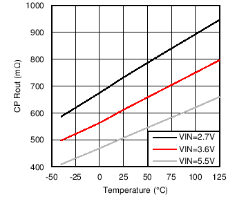 Figure 6. Charge Pump ROUT vs Temperature
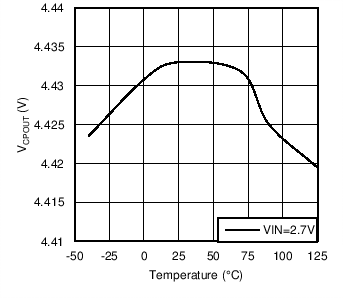 Figure 8. Charge Pump 2X Mode VCPOUT vs Temperature
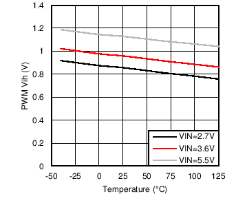 Figure 10. PWM VIH vs Temperature
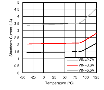 Figure 3. Shutdown IQ vs Temperature
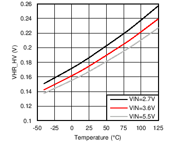 Figure 5. VHR_HV vs Temperature
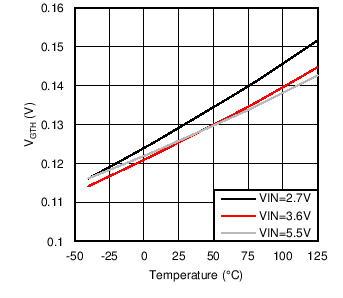 Figure 7. Low Voltage LED VGTH vs Temperature
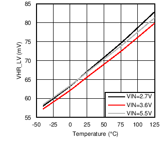 Figure 9. VHR_LV vs Temperature
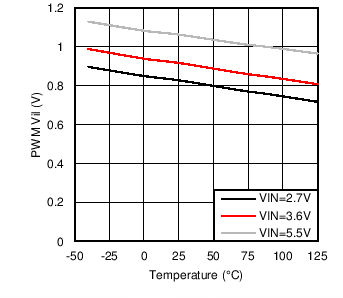 Figure 11. PWM VIL vs Temperature