SNVS867 June 2014 LM3633
PRODUCTION DATA.
- 1 Features
- 2 Applications
- 3 Description
- 4 Revision History
- 5 Pin Configuration and Functions
- 6 Specifications
-
7 Detailed Description
- 7.1 Overview
- 7.2 Functional Block Diagram
- 7.3 Feature Description
- 7.4
Device Functional Modes
- 7.4.1
High-Voltage LED Control
- 7.4.1.1 High-Voltage Boost Converter
- 7.4.1.2 High-Voltage Current Sinks (HVLED1, HVLED2 and HVLED3)
- 7.4.1.3 High-Voltage Current String Biasing
- 7.4.1.4 Boost Switching-Frequency Select
- 7.4.1.5 Automatic Switching Frequency Shift
- 7.4.1.6 Brightness Register Current Control
- 7.4.1.7 PWM Control
- 7.4.1.8 Start-up/Shutdown Ramp
- 7.4.1.9 Run-Time Ramp
- 7.4.1.10 High-Voltage Control A/B Ramp Select
- 7.4.1.11 LED Current Mapping Modes
- 7.4.1.12 Exponential Mapping
- 7.4.1.13 Linear Mapping
- 7.4.2
Low-Voltage LED Control
- 7.4.2.1 Integrated Charge Pump
- 7.4.2.2 Charge Pump Disabled
- 7.4.2.3 Automatic Gain
- 7.4.2.4 Automatic Gain (Flying Capacitor Detection)
- 7.4.2.5 1X Gain
- 7.4.2.6 2X Gain
- 7.4.2.7 Low-Voltage Current Sinks (LVLED1 to LVLED6)
- 7.4.2.8 Low-Voltage LED Biasing
- 7.4.2.9 Brightness Register Current Control
- 7.4.2.10 LED Current Mapping Modes
- 7.4.2.11 Exponential Mapping
- 7.4.2.12 Linear Mapping
- 7.4.2.13 Start-up/Shutdown Ramp
- 7.4.2.14 Run-Time Ramp
- 7.4.3 Low-Voltage LED Pattern Generator
- 7.4.4 Fault Flags/Protection Features
- 7.4.5 I2C-Compatible Interface
- 7.4.1
High-Voltage LED Control
- 7.5 Register Descriptions
-
8 Applications and Implementation
- 8.1 Application Information
- 8.2
Typical Application
- 8.2.1 Design Requirements
- 8.2.2
Detailed Design Procedure
- 8.2.2.1 Boost Converter Maximum Output Power (Boost)
- 8.2.2.2 Boost Inductor Selection
- 8.2.2.3 Output Capacitor Selection
- 8.2.2.4 Schottky Diode Selection
- 8.2.2.5 Input Capacitor Selection
- 8.2.2.6 Maximum Output Power (Charge Pump)
- 8.2.2.7 Charge Pump Flying Capacitor Selection
- 8.2.2.8 Charge Pump Output Capacitor Selection
- 8.2.2.9 Charge Pump Input Capacitor Selection
- 8.2.3 Application Performance Plots
- 8.3 Initialization Set Up
- 9 Power Supply Recommendations
- 10Layout
- 11Device and Documentation Support
- 12Mechanical, Packaging, and Orderable Information
Package Options
Mechanical Data (Package|Pins)
- YFQ|20
Thermal pad, mechanical data (Package|Pins)
Orderable Information
7 Detailed Description
7.1 Overview
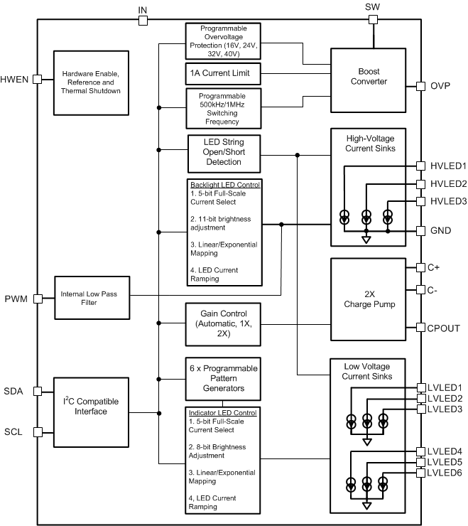
The LM3633 provides the power for three high-voltage LED strings and six low-voltage LEDs. The three high-voltage LED strings are powered from an integrated boost converter. The six low-voltage LEDs are powered from an integrated 2X charge pump. The device is programmable over an I2C-compatible interface. Additional features include a Pulse Width Modulation (PWM) input for content adjustable brightness control and 6 programmable pattern generators for RGB and indicator blinking functions on the low-voltage LEDs.
7.2 Functional Block Diagram
7.3 Feature Description
7.3.1 Control Bank Mapping
Control of the LM3633’s current sinks is not done directly, but through the programming of Control Banks. The current sinks are then assigned to the programmed Control Bank. This allows a wide variety of current control possibilities where LEDs can be grouped and controlled via specific Control Banks (see Figure 12 and Figure 17).
7.3.1.1 High-Voltage Control Banks (A and B)
There are 2 high-voltage control banks (A and B). All three high-voltage current sinks can be assigned to either Control Bank A or Control Bank B. Assigning all three current sinks to the same control bank allows for better LED current matching. Assigning a current sink to a different control bank allows for independent current sink programming. The high-voltage control bank mapping is done via bits [2:0] of the HVLED Current Sink Output Configuration register (see Table 5).
7.3.1.2 Low-Voltage Control Banks (C, D, E, F, G, and H)
There are 6 low-voltage control banks (C, D, E, F, G, and H). LVLED1 to LVLED3 can be assigned to control bank C or can be assigned to independent control banks (LVLED2 to Control Bank D and LVLED3 to Control Bank E). LVLED4 to LVLED6 can be assigned to control bank F or can be assigned to independent control banks (LVLED5 to Control Bank G and LVLED6 to Control Bank H). Assigning low-voltage current sinks to the same control bank allows for the best matching between LEDs. Assigning low-voltage current sinks to different control banks allows for each current sink to be programmed with different current levels. When the pattern generator is disabled the low-voltage ramp up/down times (Start-up/Shutdown and Run-Time) are controlled by the LVLED Controls C to E and Controls F to H Ramp Time register (see Table 11).
7.3.2 Pattern Generator
The LM3633 contains 6 independently programmable pattern generators for each low-voltage control bank. Each pattern generator can have its own separate pattern: delays from turnon, high and low-current settings, and pattern high and low times. There are two sets of rise and fall time control registers. One set is assigned to Control Banks C to E and the other set is assigned to Control Banks F to H. All other settings are independent (see Figure 17).
7.3.3 PWM Input
The PWM input which can be assigned to either of the high-voltage control banks. When assigned to a control bank, the programmed current in the control bank becomes a function of the duty cycle (DPWM) at the PWM input and the control bank brightness setting. When PWM is disabled, DPWM is equal to one.
7.3.4 HWEN Input
HWEN is the global hardware enable to the LM3633. HWEN must be pulled high to enable the device. HWEN is a high-impedance input so it cannot be left floating. When HWEN is pulled low, the LM3633 is placed in shutdown, and all the registers are reset to their default state.
7.3.5 Thermal Shutdown
The LM3633 contains a thermal shutdown protection. In the event the die temperature reaches 140°C (typ), the boost, charge pump, and current sinks shut down until the die temperature drops to typically 125°C (typ).
7.4 Device Functional Modes
7.4.1 High-Voltage LED Control
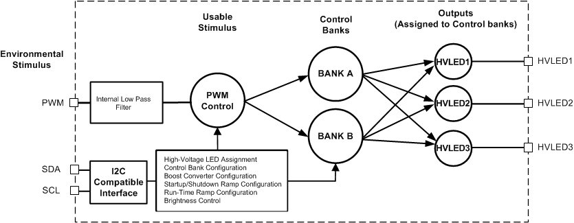 Figure 12. High-Voltage Functional Control Diagram
7.4.1.1 High-Voltage Boost Converter
The high-voltage boost converter provides power for the three high-voltage current sinks (HVLED1, HVLED2 and HVLED3). The boost circuit operates using a 4.7-µH to 22-µH inductor and a 1-µF output capacitor. The selectable 500-kHz or 1-MHz switching frequency allows for use of small external components and provides for high boost-converter efficiency. HVLED1, HVLED2, and HVLED3 feature an adaptive current regulation scheme where the feedback point (HVLED1, HVLED2, and HVLED3) regulates the LED headroom voltage to VHR_HV. When there are different voltage requirements in the high-voltage LED strings (string mismatch), the LM3633 regulates the feedback point of the highest voltage string to VHR_HV and drops the excess voltage of the lower-voltage string across the lower string(s) current sink.
7.4.1.2 High-Voltage Current Sinks (HVLED1, HVLED2 and HVLED3)
HVLED1, HVLED2, and HVLED3 control the current in the high-voltage LED strings as configured by Control Bank A or Control Bank B. Each Control Bank has 5-bit full-scale current programmability and 11-bit brightness control. High-voltage current sinks are assigned to a control bank through the HVLED Current Sink Output Configuration register (see Table 5).
7.4.1.3 High-Voltage Current String Biasing
Each high-voltage current string can be powered from the LM3633 boost output (COUT) or from an external source. The feedback enable bits (HVLED Current Sink Feedback Enables register bits [2:0]) determine where the high-voltage current string anodes are connected. When set to '1' (default) the high-voltage current sink inputs are included in the boost feedback loop. This allows the boost converter to adjust its output voltage to maintain the LED headroom voltage VHR_HV at the current sink input.
When powered from alternate sources the feedback enable bits should be set to '0'. This removes the particular current sink from the boost feedback loop. In these configurations the application must ensure that the headroom voltage across the high-voltage current sink is high enough to prevent the current sink from going into dropout (see the Figure 63 for data on the high-voltage LED current vs VHR_HV).
Setting the HVLED Current Sink Feedback Enables register bits also determines triggering of the shorted high-voltage LED String Fault flag (see Fault Flags/Protection Features section).
7.4.1.4 Boost Switching-Frequency Select
The LM3633 boost converter has two switching frequency settings. The switching frequency setting is controlled via the Boost Frequency Select bit (bit 0 in the Boost Control register). Operating at the 500-kHz switching frequency results in better efficiency under lighter load conditions due to the decreased switching losses. In this mode the inductor must be between 10 µH and 22 µH. Operating at the 1-MHz switching frequency results in better efficiency under higher load conditions due to in lower conduction losses in the MOSFETs and inductor. In this mode the inductor can be between 4.7 µH and 22 µH.
7.4.1.5 Automatic Switching Frequency Shift
The LM3633 has an automatic frequency-select mode (bit 3 in the Boost Control register) to optimize the frequency vs load dependent losses. In Auto-Frequency mode the boost converter switching frequency is changed based on the high-voltage LED current. The threshold (Control A and Control B brightness code) at which the frequency switchover occurs is programmable via the Auto-Frequency Threshold register. The Auto-Frequency Threshold register contains an 8-bit code which is compared to the 8 MSBs of the brightness code. When the brightness code is greater than the Auto-Frequency Threshold value the boost converter switching frequency is 1 MHz. When the brightness code is less than or equal to the Auto-Frequency Threshold register the boost converter switching frequency is 500 kHz. The default value in the Auto-Frequency Threshold register is set for the default full-scale current setting (20.2 mA).
Figure 13 shows the LED efficiency improvement (3p5s LED configuration with a 4.7-μH inductor) when the auto-frequency feature is enabled. When the LED brightness is less than or equal to 0x6C, the switching frequency is 500 kHz, and it improves the LED efficiency by up to 6%. When the LED brightness is greater than 0x6C, the switching frequency is 1 MHz, and it improves LED efficiency by up to 2.2%.
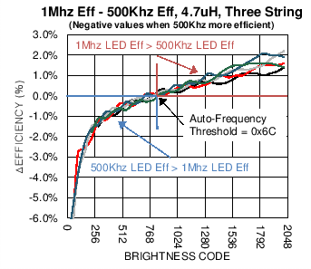 Figure 13. Auto-Frequency Boost Efficiency Improvement
Table 1 summarizes the general recommendations for auto-frequency threshold setting vs inductance values and LED string configurations. These are general recommendations — the optimum auto-frequency threshold setting should be evaluated for each application
Table 1. Auto-Frequency Threshold Settings
| THREE STRING | TWO STRING | |||||
|---|---|---|---|---|---|---|
| INDUCTOR (µH) | AUTO-FREQUENCY THRESHOLD | PEAK EFFICIENCY IMPROVEMENT (%) | PEAK CONFIGURATION | AUTO-FREQUENCY THRESHOLD | PEAK EFFICIENCY IMPROVEMENT(%) | PEAK CONFIGURATION |
| 4.7 | 6C | 2.2 | 3p5s | AC | 1.1 | 2p6s |
| 10 | 74 | 1.7 | 3p4s | B4 | 1.3 | 2p5s |
| 22 | 7C | 0.7 | 3p3s | BC | 0.7 | 2p4s |
7.4.1.6 Brightness Register Current Control
The Brightness Register Current Control allows simple user-adjustable current control by writing directly to the appropriate control bank brightness register. The current for Control Bank A and B is a function of the full-scale LED current, the 11-bit code in the respective brightness register, and the PWM input duty cycle (if PWM is enabled). The Control Bank A and B brightness should always be written with LSBs first and MSBs last.
7.4.1.6.1 8-Bit Control (Preferred)
The preferred operating mode is to control the high-voltage LED brightness by setting the Control Bank LSB register (3 LSBs) to zero, using only the Control Bank MSB register (8 MSBs). In 8-bit control mode the LM3633 controls the 3 LSBs to ramp the high-voltage LED current using all 11 bits.
7.4.1.6.2 11-Bit Control
In this mode of operation, both Control Bank LSB and MSB registers must be written whenever a change in Brightness is required. The high-voltage LED current does not change until the Control Bank MSB register is written. If the brightness change affects only the 3 LSBs, the Control Bank MSB register (8 MSBs) must be rewritten to change the high-voltage LED current.
7.4.1.7 PWM Control
The LM3633 PWM input can be enabled for Control Bank A or B (see Table 21). Once enabled, the LED current becomes a function of the code in the Control Brightness registers and the PWM input-duty cycle.
The PWM input accepts a logic level voltage and internally filters it to an analog-control voltage. This results in a linear response of duty cycle to current, where 100% duty cycle corresponds to the programmed brightness code multiplied by the Full-Scale Current setting.
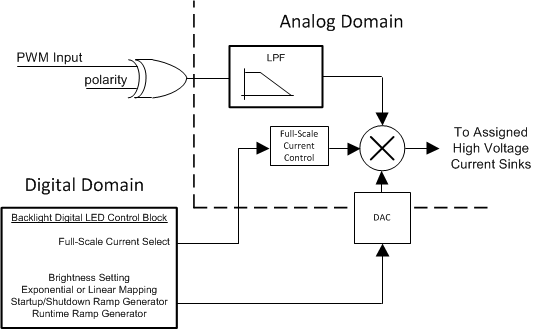 Figure 14. PWM Input Architecture
7.4.1.7.1 PWM Input Frequency Range
The usable input frequency range for the PWM input is governed on the low end by the cutoff frequency of the internal low-pass filter (540 Hz, Q = 0.33) and on the high end by the propagation delays through the internal logic. For frequencies below 2 kHz the current ripple begins to become a larger portion of the DC LED current. Additionally, at lower PWM frequencies the boost output voltage ripple increases, causing a non-linear response from the PWM duty cycle to the average LED current due to the response time of the boost and current-sink dropout. For the best response of current vs. duty cycle, the PWM input frequency should be kept between 2 kHz and 100 kHz.
7.4.1.7.2 PWM Input Polarity
The PWM Input can be set for active low polarity, where the LED current is a function of the negative duty cycle. This is set via the PWM Configuration register (see Table 21).
7.4.1.7.3 PWM Zero Detection
The LM3633 incorporates a feature to detect when the PWM input is near zero. When this feature is enabled the minimum PWM input pulse must be greater than tPWM (see Electrical Characteristics). Bit 3 in the PWM Configuration register is used to enable or disable PWM zero detection.
7.4.1.8 Start-up/Shutdown Ramp
The high-voltage LED start-up and shutdown ramp times are independently programmable in the Control A and Control B Start-Up/Shutdown Ramp Time register (see Table 7). There are 16 different start-up and 16 different shutdown times. The start-up times can be programmed independently from the shutdown times, but each Control bank is not independently programmable.
The start-up ramp time is the period from when the Control Bank is enabled to when the LED current reaches its initial set point. The shutdown ramp time is the period from when the Control Bank is disabled to when the LED current reaches 0.
7.4.1.9 Run-Time Ramp
Current ramping from one brightness level to the next is programmed via the Control A and Control B Run-Time Transition Time register (see Table 9). There are 16 different ramp-up times and 16 different ramp-down times. The ramp-up time can be programmed independently from the ramp-down time, but each Control Bank cannot be independently programmed. For example, programming a ramp-up or ramp-down time is a global setting for all high-voltage LED Control Banks.
7.4.1.10 High-Voltage Control A/B Ramp Select
The LM3633 provides three options for configuring Control A and Control B ramp times. When the run-time ramp select bits are set to 00 the control bank uses both the start-up/shutdown and run-time ramp times. When the run-time ramp select bits are set to 01 the control bank uses the start-up/shutdown ramp times for both startup/shutdown and run-time. When the run-time ramp select bits are set to 1x the control bank uses a zero µsec run-time ramp.
7.4.1.11 LED Current Mapping Modes
All control banks can be programmed for either exponential or linear mapping modes (see Figure 19). These modes determine the transfer characteristic of backlight code to LED current. Independent mapping of Control Bank A and B is not allowed; both banks use the same mapping mode.
7.4.1.12 Exponential Mapping
In Exponential Mapping Mode the current ramp (either up or down) appears to the human eye as a more uniform transition than the linear ramp. This is due to the logarithmic response of the eye.
7.4.1.12.1 8-Bit Code Calculation
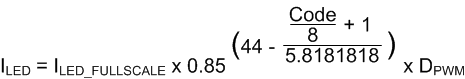
In 8-bit Exponential Mapping Mode the brightness code-to-backlight current transfer function is given by the equation:
Where ILED_FULLSCALE is the full-scale LED current setting (see Table 13), Code is the 8-bit brightness code in the Control Brightness MSB register and DPWM is the PWM Duty Cycle.
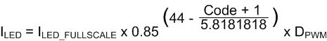
7.4.1.12.2 11-Bit Code Calculation
In 11-bit Exponential Mapping Mode the brightness code-to-backlight current transfer function is given by the equation:
Where ILED_FULLSCALE is the full-scale LED current setting (see Table 13), Code is the 11-bit brightness code in the Control Brightness MSB and LSB registers and DPWMis the PWM Duty Cycle.
7.4.1.13 Linear Mapping
In Linear Mapping Mode the brightness code-to-backlight current has a linear relationship.
7.4.1.13.1 8-Bit Code Calculation
In Linear Mapping Mode the brightness code-to-backlight current has a linear relationship and follows the equation:
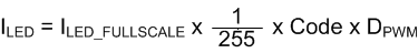
Where ILED_FULLSCALE is the full-scale LED current setting, Code is the 8-bit brightness code in the Control Brightness MSB register and DPWMis the PWM Duty Cycle.
7.4.1.13.2 11-Bit Code Calculation
In Linear Mapping Mode the brightness code-to-backlight current has a linear relationship and follows the equation:
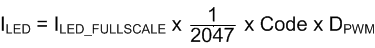
Where ILED_FULLSCALE is the full-scale LED current setting, Code is the 11-bit brightness code in the Control Brightness MSB and LSB registers and DPWMis the PWM Duty Cycle.
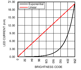 Figure 15. LED Current Mapping Modes (8-bit)
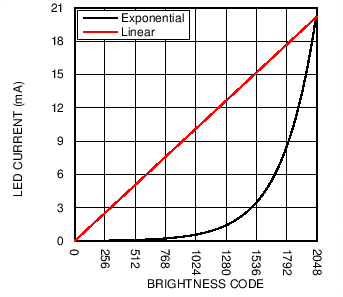 Figure 16. LED Current Mapping Modes (11-bit)
7.4.2 Low-Voltage LED Control
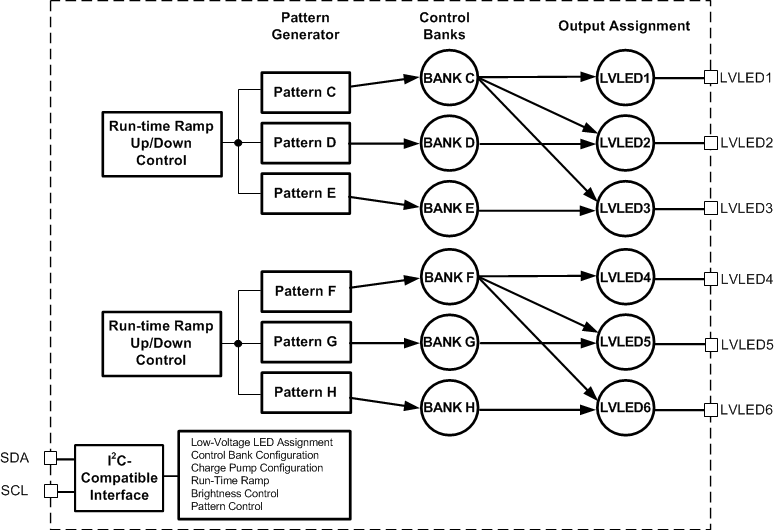 Figure 17. Low-Voltage LED Functional Control Diagram
7.4.2.1 Integrated Charge Pump
The LM3633 features an integrated (2X/1X) charge pump capable of supplying LVLED1 to LVLED6 current. The fixed 1-MHz switching frequency allows for use of tiny 1-µF ceramic flying capacitors (CP) and output capacitor (CPOUT). The charge pump can supply the power for the low-voltage LEDs connected to LVLED1 to LVLED6 and can operate in 4 different modes: disabled, automatic gain, 1X gain, or 2X gain (see Figure 18).
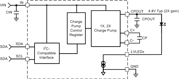 Figure 18. Integrated Charge Pump
7.4.2.2 Charge Pump Disabled
With the charge pump disabled, the path from IN to CPOUT is high impedance. Additionally, with the charge pump disabled, the low-voltage current sinks can still be active, thus allowing the low-voltage LEDs to be biased from external sources (see Low-Voltage LED Biasing section). Disabling the charge pump also has no influence on the state of the low-voltage current sinks. For instance, if a low-voltage current string is set to have its anode connected to CPOUT, and the charge pump is disabled, the current sink continues to try to sink current.
7.4.2.3 Automatic Gain
In Automatic Gain Mode the charge-pump-gain transition is actively selected to maintain LED current regulation in the CPOUT-connected, low-voltage current sinks. At higher input voltages the charge pump operates in Pass Mode (1x gain) allowing the voltage at CPOUT to track the input voltage. As VIN drops, the voltage on the low-voltage current sink(s) drops also. Once any of the active, CPOUT-connected, low-voltage current sink input voltages reach VHR_LV (see Electrical Characteristics), the charge pump automatically switches to a gain of 2x thus preventing dropout (see 2X Gain). Once the charge pump switches over to 2X gain it remains in 2X gain until the active low-voltage current sinks are turned off (enable bit or brightness code 0), even if the current sink input voltage goes above the switch over threshold.
7.4.2.4 Automatic Gain (Flying Capacitor Detection)
In Automatic Gain Mode the LM3633 starts up and automatically detects if there is a flying capacitor (CP) connected between C+ and C−. If there is, Automatic Gain Mode operates normally. If the detection circuitry does not detect a connected flying capacitor, the LM3633 automatically switches to 1X Gain mode.
7.4.2.5 1X Gain
In 1X Gain Mode the charge pump passes VIN directly through to the output capacitor (CPOUT). There is a resistive drop between IN and CPOUT in the 1X Gain Mode (typically 1.1 Ω) which should be accounted for when determining the headroom requirement for the low-voltage current sinks. In forced 1X Gain Mode the charge pump does not switch; thus, the CP and CPOUT can be omitted from the circuit.
7.4.2.6 2X Gain
In 2X Gain Mode the internal charge pump doubles VIN and post-regulates CPOUT to, typically, 4.4 V. This allows for biasing LEDs whose forward voltages are greater than the input supply (VIN).
7.4.2.7 Low-Voltage Current Sinks (LVLED1 to LVLED6)
Low-voltage current sinks LVLED1 to LVLED6 each provide the current for a single LED as configured via Control Banks C to H. Each control bank has 8-bit brightness control and 5-bit full-scale current programmability. The low-voltage current sinks can be controlled directly through a dedicated brightness register or with different blinking patterns via the 6 internal pattern generators. Configuration of the low-voltage current sinks is done through the low-voltage Control Bank C to H (LVLED1, LVLED2, and LVLED3 to Control Bank C to E and LVLED4, LVLED5, and LVLED6 to Control Bank F to H). (See Table 6.)
7.4.2.8 Low-Voltage LED Biasing
Each low-voltage LED can be powered from the LM3633 charge pump output (CPOUT) or from an external source. When powered from CPOUT the feedback enable bit (LVLED Current Sink Feedback Enables Register bits [5:0]) for that particular low-voltage current sink must be set to '1' (default). This allows for the specific low-voltage current sink to have control over the charge pumps gain control (see Automatic Gain section).
When powered from alternate sources (such as VIN) the feedback enable bit for the particular low-voltage current sink must be set to '0'. This removes the particular current sink from the charge pump feedback loop. In these configurations the application must ensure that the headroom voltage across the low-voltage current sink is high enough to prevent the low-voltage current sinks from going into dropout (see Figure 64 for data on the low-voltage LED current vs headroom voltage).
The LVLEDX feedback enable bits also determine how the shorted low-voltage LED String fault flag is triggered (see Fault Flags/Protection Features).
7.4.2.9 Brightness Register Current Control
The LM3633 features brightness register current control for simple user-adjustable current control set by writing directly to the appropriate Control Bank Brightness Registers. The current for the low-voltage LED Control Bank C to H is a function of the full-scale LED current and the 8-bit code in the respective brightness register. The control bank brightness register code represents the percentage of the full-scale LED current. This percentage of full-scale current is different depending on the selected mapping mode (see Table 12).
7.4.2.10 LED Current Mapping Modes
All control banks can be programmed for either exponential or linear mapping modes (see Figure 19). These modes determine the transfer characteristic of brightness code to LED current. All low-voltage control banks use the same mapping mode.
7.4.2.11 Exponential Mapping
In Exponential Mapping Mode the current ramp (either up or down) appears to the human eye as a more uniform transition than the linear ramp. This is due to the logarithmic response of the eye.
In Exponential Mapping Mode the brightness code-to-current transfer function is given by the equation:
Where ILED_FULLSCALE is the full-scale LED current setting (see Table 13) and Code is the brightness code in the brightness register.
7.4.2.12 Linear Mapping
In Linear Mapping Mode the brightness code-to-current has a linear relationship and follows the equation:
Where ILED_FULLSCALE is the full-scale LED current setting and Code is the brightness code in the brightness register.
Figure 19. LED Current Mapping Modes
7.4.2.13 Start-up/Shutdown Ramp
The start-up and shutdown ramp times are independently programmable in the Control C to Control H Start-Up/Shutdown Ramp-Time registers (see Table 8). There are 8 different start-up and 8 different shutdown times. The start-up times can be programmed independently from the shutdown times. The start-up ramp time is from when the Control Bank is enabled to when the LED current reaches its initial set point. The shutdown ramp time is from when the Control Bank is disabled to when the LED current reaches 0.
7.4.2.14 Run-Time Ramp
Current ramping from one brightness level to the next is programmed via the Control C to E and Control F to H Ramp-Time registers (see Table 11). There are 8 different ramp-up times and 8 different ramp-down times. The ramp-up time can be programmed independently from the ramp-down time, but each Control Bank cannot be independently programmed. There is one ramp time register which is common to Control Bank C to E and one ramp time register which is common to Control Bank F to H. This register sets the ramp-up and ramp-down times for both direct brightness control and pattern generator modes of operation.
7.4.3 Low-Voltage LED Pattern Generator
The LM3633 contains 6 programmable pattern generators (one for each low-voltage control bank). Each pattern generator has the ability to drive a unique programmable pattern. Each pattern generator has its own set of registers available for pattern programming. The programmable patterns are : delay time, high period, low period, high brightness, and low brightness (see Figure 20). The ramp-up and ramp-down times are controlled by the Control C to E and Control F to H Ramp-Time register. (See Table 11.)
 Figure 20. Pattern Generator Timing
7.4.3.1 Delay Time
The delay time (tDELAY) is the delay from when the pattern is enabled to when the LED current begins ramping up in the control bank assigned current source(s). The pattern starts when the respective Control Bank Enable register is written high if the Pattern Generator is enabled. There is one tDELAY register for each pattern generator (6 total). The selectable times are programmed with the lower 6 bits of the tDELAY registers. The times are split into 2 groups where codes 0x00 to 0x3C are short durations from 16.384 ms (code 0x00) up to 999.424 ms (code 0x3C) or 16.384 ms/bit. The higher codes (0x3D to 0x7F) select tDELAY from 1130.496 ms up to 9781.248 ms, or 131.072 ms/bit (see Table 27).
7.4.3.2 Rise Time
The LED current rise time (tRISE) is the time the LED current takes to move from the low-current brightness level (ILOW) to the high-current brightness level (IHIGH). The rise time of the LED current (tRISE) is set via the Control C to E and Control F to H Ramp-Time registers. There are 8 available ramp-up time settings (see Table 11). There is one ramp-time register which is common to Control Bank C to E and one ramp-time register which is common to Control Bank F to H.
7.4.3.3 Fall Time
The LED current fall time (tFALL) is the time the LED current takes to move from the high-current brightness level (IHIGH) to the low-current brightness level (ILOW). The fall time of the LED current (tFALL) is set via the Control C to E and Control F to H Ramp Time registers. There are 8 available ramp-down settings (see Table 11). There is one ramp-time register which is common to Control Bank C to E and one ramp-time register which is common to Control Bank F to H.
7.4.3.4 High Period
The LED current high period (tHIGH) is the duration that the LED pattern spends at the high LED current set point (tHIGH). The tHIGH times are programmed via the Pattern Generator High-Time registers. The programmable times are broken into 2 groups. The first set (from code 0x00 to 0x3C) increases the tHIGH time in steps of 16.384 ms. The second set (from code 0x3D to 0x7F) increases the tHIGH time in steps of 131.072 ms (see Table 29).
7.4.3.5 Low Period
The LED current low period (tLOW) is the duration that the LED current spends at the low LED current set point (ILOW). The tLOW times are programmed via the Pattern Generator Low-Time registers. There are 256 tLOW settings that are broken into 3 groups of linearly increasing times. The first set (from code 0x00 to 0x3C) increases the tLOW time in steps of 16.384 ms. The second set (from code 0x3D to 0x7F) increases the tLOW time in steps of 131.072 ms. The third set (from code 0x80 to 0xFF) increases the tLOW time in steps of 524.288 ms (see Table 28).
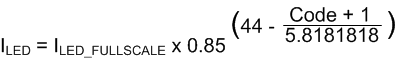
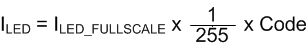
7.4.3.6 Low-Level Brightness
The LED current low brightness level (ILOW) is the LED current set point that the pattern rests at during the tLOW period. This level is set via the Pattern Generator Low-Level Brightness registers (BREGL_C to BREGL_H). The brightness level has 8 bits of programmability. ILOW is a function of the Control Bank full-scale current setting and the code in the Pattern Generator Low-Level Brightness registers.
For exponential mapping ILOW is:
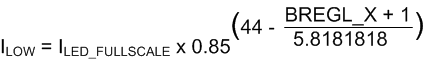
For linear mapping ILOW is:
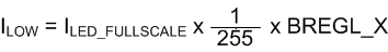
BREGL_X is the Pattern Generator Low-Level Brightness Register setting for the specific Control Bank.
7.4.3.7 High-Level Brightness
The LED current high brightness level (IHIGH) is the LED current set point that the pattern rests at during the tHIGH period. This high-current level is set via the Control Banks Brightness Register (BREGH_C to BREGH_H). The brightness level has 8 bits of programmability. IHIGH is a function of the Control Bank full-scale current setting and the code in the Control Banks Brightness Register, prior to the Mapping Mode selected.
For exponential mapping IHIGH is:
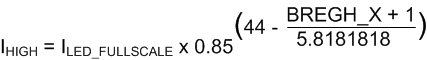
For linear mapping IHIGH is:
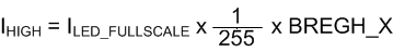
BREGH_X is the Control Banks Brightness Register setting for the specific Control Bank.
7.4.4 Fault Flags/Protection Features
The LM3633 contains both an LED open-fault and LED short-fault detection. These fault detections are designed to be used in production-level testing and not during normal operation. For the fault flags to operate they must be enabled via the LED Fault Enable Register (see Table 35). The Open LED String (HVLED), Shorted LED String (HVLED), Open LED (LVLED), and Shorted LED (LVLED) sections detail proper procedure for reading back open and short faults in both the high-voltage LED and low-voltage LED strings.
7.4.4.1 Open LED String (HVLED)
An open LED string is detected when the voltage at the input to any active high-voltage current sink has fallen below 200 mV, and the boost output voltage has hit the OVP threshold. This test assumes that the HVLED string being detected for an open is connected to the LM3633 boost output (COUT+) (see Table 31). For an HVLED string not connected to the LM3633 boost output voltage, but connected to another voltage source, the boost output does not trigger the OVP flag. In this case an open LED string is not detected.
The procedure for detecting an open fault in the HVLED current sinks (provided they are connected to the boost output voltage) is:
- Apply power to the LM3633
- Enable Open Fault (Register 0xB4, bit [0] = 1)
- Assign HVLED1, HVLED2 and HVLED3 to Bank A (Register 0x10, Bits [2:0] = (0, 0, 0)
- Set the start-up ramp times to the fastest setting (Register 0x12 = 0x00)
- Set Bank A full-scale current to 20.2 mA (Register 0x20 = 0x13)
- Configure HVLED1, HVLED2, and HVLED3 for LED string anode connected to COUT (Register 0x28, bits[2:0] = (1,1,1))
- Set Bank A brightness to maximum (Register 0x41 = 0xFF)
- Enable Bank A (Register 0x2B Bit[0] = 1
- Wait 4 ms
- Read back bits[2:0] of register 0xB0. Bit [0] = 1 (HVLED1 open). Bit [1] = 1 (HVLED2 open). Bit [2] = 1 (HVLED3 open)
- Disable all banks (Register 0x2B = 0x00)
7.4.4.2 Shorted LED String (HVLED)
The LM3633 features an LED short-fault flag indicating one or more of the HVLED strings have experienced a short. The method for detecting a shorted HVLED strings is if the current sink is enabled and the string voltage (VOUT - VHVLED1/2/3) falls to below (VIN – 1 V). This test must be performed on one HVLED string at a time. Performing the test with both current sinks enabled can result in a faulty reading if one of the strings is shorted and the others are not.
The procedure for detecting a short in an HVLED string is:
- Apply power to the LM3633
- Enable Short Fault (Register 0xB4, bit [1] = 1)
- Enable Feedback on the HVLED Current Sinks (Register 0x28, bits[2:0] = (1,1,1))
- Assign HVLED1 to Bank A (Register 0x10, Bits [2:0] = (1, 1, 0)
- Set the start-up ramp times to the fastest setting (Register 0x12 = 0x00)
- Set Bank A full-scale current to 20.2 mA (Register 0x20 = 0x13)
- Set Bank A brightness to max (Register 0x41 = 0xFF)
- Enable Bank A (Register 0x2B Bit[0] = 1)
- Wait 4 ms
- Read back bits[0] of register 0xB2. 1 = HVLED1 short.
- Disable all banks (Register 0x2B = 0x00)
- Repeat the procedure for the HVLED2 and HVLED3 strings
7.4.4.3 Open LED (LVLED)
The LM3633 features an open-LED-fault flag indicating one or more of the active low-voltage LED strings are open. An open in a low-voltage LED string is flagged if the voltage at the input to any active low-voltage current sink goes below VHR_LV (typically 80 mV).
Since the open LED detect is flagged when any active current sink input falls below VHR_LV, certain configurations can result in falsely triggering an open. These include:
- LED anode is tied to CPOUT, charge pump is in 1X gain, and VIN drops low enough to bring any active LVLED current sink below VHR_LV.
- LED anodeis not tied to CPOUT and VLED_ANODE goes low enough to bring any active LVLED current sink below VHR_LV.
The following list describes a test procedure that can be used in detecting an open in the LVLED strings:
- Apply power to the LM3633
- Enable Open Fault (Register 0xB4, bit [0] = 1)
- Assign LVLED1, LVLED2, and LVLED3 to Bank C and LVLED4, LVLED5, and LVLED6 to Bank F (Register 0x11 = 0x00)
- Set the start-up ramp times to the fastest setting (Registers 0x14 and 0x17 = 0x00)
- Set Bank C and Bank F full-scale current to 20.2 mA (Registers 0x22 and 0x25 = 0x13)
- Configure all LVLED strings for Anode connected to CPOUT (register 0x29 bits[5:0]=1)
- Force the Charge Pump into 2X gain (Register 0x2A Bits[2:1] = 11). Ensure that CPOUT and CP are in the circuit and that (VCPOUT is > VFLVLED + VHR_LV)
- Set Bank C and Bank F brightness to max (Registers 0x42 and 0x45 = 0xFF)
- Enable Bank C and Bank F (Register 0x2B Bits[5,2] = 1)
- Wait 4 ms
- Read back bits[5:0] of register 0xB1 (1 indicates an open, and a 0 indicates normal operation (see Table 32))
- Disable all banks (Register 0x2B = 0x00)
7.4.4.4 Shorted LED (LVLED)
The LM3633 features an LED short-fault flag indicating when any active low-voltage LED is shorted (Anode to Cathode). A short in a low-voltage LED is determined when the LED voltage (VCPOUT - VHR_LV) falls below 1 V.
A procedure for determining a short in an LVLED string is detailed below:
- Apply Power
- Enable Short Fault (Register 0xB4, bit [1] = 1)
- Assign LVLED1, LVLED2, and LVLED3 to Bank C and LVLED4, LVLED5, and LVLED6 to Bank F (Register 0x11 = 0x00)
- Set the start-up ramp times to the fastest setting (Registers 0x14 and 0x17 = 0x00)
- Set Bank C and Bank F full-scale current to 20.2 mA (Registers 0x22 and 0x25 = 0x13)
- Enable Feedback on the LVLED Current Sinks (Register 0x29 = 0x3F)
- Set Charge Pump to 1X gain (Register 0x2A = 0x40)
- Set Bank C and Bank F brightness to max (Register 0x42 and 0x45 = 0xFF)
- Enable Bank C and Bank F(Register 0x2B Bits[5,2] = 1)
- Wait 4 ms
- Read bits[5:0] from register 0xB3. A 1 indicates short, and a 0 indicates normal operation (see Table 34).
- Disable all banks (Register 0x2B = 0x00)
7.4.4.5 Overvoltage Protection (Inductive Boost)
The overvoltage protection threshold (OVP) on the LM3633 has 4 different programmable options: 16 V, 24 V, 32 V, and 40 V. The OVP protects the device and associated circuitry from high voltages in the event a high-voltage LED string becomes open. During normal operation, the LM3633 inductive boost converter boosts the output up so as to maintain VHR at the active, high-voltage (COUT connected) current sink inputs. When a high-voltage LED string becomes open, the feedback mechanism is broken, and the boost converter over-boosts the output. When the output voltage reaches the OVP threshold the boost converter stops switching, thus allowing the output node to discharge. When the output discharges to VOVP minus 1 V, the boost converter begins switching again. The OVP sense is at the OVP pin, so this pin must be connected directly to the inductive boost output capacitor positive pin.
For high-voltage current sinks that have the HVLED Current Sink Feedback Enables setting such that the high-voltage current sinks anodes are not connected to COUT (feedback is disabled), the overvoltage sense mechanism is not in place to protect the input to the high-voltage current sink. In this situation the application must ensure that the voltage at HVLED1, HVLED2, or HVLED3 does not exceed 40 V.
The default setting for OVP is set at 16 V. For applications that require higher than 16 V at the boost output, the OVP threshold must be programmed to a higher level after power up.
7.4.4.6 Current Limit (Inductive Boost)
The NMOS switch current limit for the LM3633 inductive boost is set at 1 A (typ). When the current through the LM3633 NFET switch hits this overcurrent protection threshold (OCP), the device turns the NFET off, and the inductor’s energy is discharged into the output capacitor. Switching is then resumed at the next cycle. The current limit protection circuitry can operate continuously each switching cycle. The result is that during high-output power conditions the device can run continuously in current limit. Under these conditions the LM3633 inductive boost converter stops regulating the headroom voltage across the high-voltage current sinks. This results in a drop in the LED current.
7.4.4.7 Current Limit (Charge Pump)
The LM3633 charge pump output current limit is set high enough so that the device supports 29.8 mA (maximum full-scale current) in all LVLED current sinks. (This is typically 29.5 mA x 6 = 179 mA.) For 1X gain the output current limit is typically 350 mA (VIN = 3.6 V). For 2X gain the current limit is typically 240 mA (output referred), with a typical limit on the input current of 480 mA. Figure 67 and Figure 68 detail the charge pump current limit vs VIN at both 1X and 2X gain settings.
7.4.5 I2C-Compatible Interface
7.4.5.1 Start and Stop Conditions
The LM3633 is controlled via an I2C-compatible interface. START and STOP conditions classify the beginning and the end of the I2C session. A START condition is defined as SDA transitioning from HIGH to LOW while SCL is HIGH. A STOP condition is defined as SDA transitioning from LOW to HIGH while SCL is HIGH. The I2C master always generates START and STOP conditions. The I2C bus is considered busy after a START condition and free after a STOP condition. During data transmission the I2C master can generate repeated START conditions. A START and a repeated START condition are equivalent function-wise. The data on SDA must be stable during the HIGH period of the clock signal (SCL). In other words, the state of SDA can only be changed when SCL is LOW.
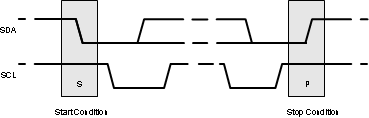 Figure 21. Start and Stop Sequences
7.4.5.2 I2C-Compatible Address
The chip address for the LM3633 is 0110110 (36h). After the START condition, the I2C master sends the 7-bit chip address followed by an eighth read or write bit (R/W). R/W = 0 indicates a WRITE, and R/W = 1 indicates a READ. The second byte following the chip address selects the register address to which the data is written. The third byte contains the data for the selected register.
7.4.5.3 Transferring Data
Every byte on the SDA line must be eight bits long, with the most significant bit (MSB) transferred first. Each byte of data must be followed by an acknowledge bit (ACK). The acknowledge related clock pulse (9th clock pulse) is generated by the master. The master releases SDA (HIGH) during the 9th clock pulse. The LM3633 pulls down SDA during the 9th clock pulse signifying an acknowledge. An acknowledge is generated after each byte has been received.
7.5 Register Descriptions
Table 2 lists the available registers within the LM3633.
Table 2. LM3633 Register Descriptions
| Name | Address | Power On Reset | Operation |
|---|---|---|---|
| Revision | 0x00 | 0x00 | Dynamic |
| Software Reset | 0x01 | 0x00 | Dynamic |
| HVLED Current Sink Output Configuration | 0x10 | 0x06 | Static |
| LVLED Current Sink Output Configuration | 0x11 | 0x36 | Static |
| Control A Start-Up/Shutdown Ramp Time | 0x12 | 0x00 | Static |
| Control B Start-Up/Shutdown Ramp Time | 0x13 | 0x00 | Static |
| Control C Start-Up/Shutdown Ramp Time | 0x14 | 0x00 | Static |
| Control D Start-Up/Shutdown Ramp Time | 0x15 | 0x00 | Static |
| Control E Start-Up/Shutdown Ramp Time | 0x16 | 0x00 | Static |
| Control F Start-Up/Shutdown Ramp Time | 0x17 | 0x00 | Static |
| Control G Start-Up/Shutdown Ramp Time | 0x18 | 0x00 | Static |
| Control H Start-Up/Shutdown Ramp Time | 0x19 | 0x00 | Static |
| Control A and Control B Runtime Ramp Time | 0x1A | 0x00 | Static |
| Control A and Control B Runtime Ramp Configuration | 0x1B | 0x00 | Static |
| Control C to E Runtime Ramp Time | 0x1C | 0x00 | Static |
| Control F to H Runtime Ramp Time | 0x1D | 0x00 | Static |
| Reserved | 0x1E | 0x33 | Static |
| Brightness Configuration | 0x1F | 0x00 | Static(4) |
| Control A Full-Scale Current Setting | 0x20 | 0x13 | Static |
| Control B Full-Scale Current Setting | 0x21 | 0x13 | Static |
| Control C Full-Scale Current Setting | 0x22 | 0x13 | Static |
| Control D Full-Scale Current Setting | 0x23 | 0x13 | Static |
| Control E Full-Scale Current Setting | 0x24 | 0x13 | Static |
| Control F Full-Scale Current Setting | 0x25 | 0x13 | Static |
| Control G Full-Scale Current Setting | 0x26 | 0x13 | Static |
| Control H Full-Scale Current Setting | 0x27 | 0x13 | Static |
| HVLED Current Sink Feedback Enable | 0x28 | 0x07 | Static |
| LVLED Current Sink Feedback Enable | 0x29 | 0x3F | Static |
| Charge Pump Control | 0x2A | 0x00 | Dynamic(1) |
| Control Bank Enables | 0x2B | 0x00 | Dynamic(4) |
| Pattern Generator Enable | 0x2C | 0x00 | Dynamic |
| Boost Control | 0x2D | 0x00 | Static |
| Auto-Frequency Threshold | 0x2E | 0xCF | Static |
| PWM Configuration | 0x2F | 0x04 | Dynamic(2) |
| Reserved | 0x30 | 0x0B | Static |
| Reserved | 0x31 | 0x00 | Static |
| Control A Brightness LSB | 0x40 | 0x00 | Dynamic(3) |
| Control A Brightness MSB | 0x41 | 0x00 | Dynamic |
| Control B Brightness LSB | 0x42 | 0x00 | Dynamic(3) |
| Control B Brightness MSB | 0x43 | 0x00 | Dynamic |
| Control C Brightness | 0x44 | 0x00 | Dynamic |
| Control D Brightness | 0x45 | 0x00 | Dynamic |
| Control E Brightness | 0x46 | 0x00 | Dynamic |
| Control F Brightness | 0x47 | 0x00 | Dynamic |
| Control G Brightness | 0x48 | 0x00 | Dynamic |
| Control H Brightness | 0x49 | 0x00 | Dynamic |
| Control C Pattern Generator Delay Time | 0x50 | 0x00 | Static |
| Control C Pattern Generator Low Time | 0x51 | 0x00 | Static |
| Control C Pattern Generator High Time | 0x52 | 0x00 | Static |
| Control C Pattern Generator Low-Level Brightness | 0x53 | 0x00 | Dynamic |
| Control D Pattern Generator Delay Time | 0x60 | 0x00 | Static |
| Control D Pattern Generator Low Time | 0x61 | 0x00 | Static |
| Control D Pattern Generator High Time | 0x62 | 0x00 | Static |
| Control D Pattern Generator Low-Level Brightness | 0x63 | 0x00 | Dynamic |
| Control E Pattern Generator Delay Time | 0x70 | 0x00 | Static |
| Control E Pattern Generator Low Time | 0x71 | 0x00 | Static |
| Control E Pattern Generator High Time | 0x72 | 0x00 | Static |
| Control E Pattern Generator Low-Level Brightness | 0x73 | 0x00 | Dynamic |
| Control F Pattern Generator Delay Time | 0x80 | 0x00 | Static |
| Control F Pattern Generator Low Time | 0x81 | 0x00 | Static |
| Control F Pattern Generator High Time | 0x82 | 0x00 | Static |
| Control F Pattern Generator Low-Level Brightness | 0x83 | 0x00 | Dynamic |
| Control G Pattern Generator Delay Time | 0x90 | 0x00 | Static |
| Control G Pattern Generator Low Time | 0x91 | 0x00 | Static |
| Control G Pattern Generator High Time | 0x92 | 0x00 | Static |
| Control G Pattern Generator Low-Level Brightness | 0x93 | 0x00 | Dynamic |
| Control H Pattern Generator Delay Time | 0xA0 | 0x00 | Static |
| Control H Pattern Generator Low Time | 0xA1 | 0x00 | Static |
| Control H Pattern Generator High Time | 0xA2 | 0x00 | Static |
| Control H Pattern Generator Low-Level Brightness | 0xA3 | 0x00 | Dynamic |
| HVLED Open Faults | 0xB0 | 0x00 | Production Test Only |
| LVLED Open Faults | 0xB1 | 0x00 | Production Test Only |
| HVLED Short Faults | 0xB2 | 0x00 | Production Test Only |
| LVLED Short Faults | 0xB3 | 0x00 | Production Test Only |
| LED Fault Enable | 0xB4 | 0x00 | Production Test Only |
Table 3.
Revision (Address 0x00)
| Bits [7:4] Not Used |
Bits [3:0] Silicon Revision |
|---|---|
| Reserved | xxxx Rev. A Silicon |
Table 4. Software Reset (Address 0x01)
| Bits [7:1] Not Used |
Bit [0] Silicon Revision |
|---|---|
| Reserved | 0 = Normal Operation 1 = Software Reset (self-clearing) |
Table 5. HVLED Current Sink Output Configuration (Address 0x10)
| Bits [7:3] Not Used |
Bit [2] HVLED3 Configuration |
Bit [1] HVLED2 Configuration |
Bit [0] HVLED1 Configuration |
|---|---|---|---|
| Reserved | 0 = Control A 1 = Control B (default) |
0 = Control A 1 = Control B (default) |
0 = Control A (default) 1 = Control B |
Table 6. LVLED Current Sink Output Configuration (Address 0x11)
| Bits [7:6] Not Used |
Bit [5] LVLED6 Configuration |
Bit [4] LVLED5 Configuration |
Bit [3] Not Used |
Bit [2] LVLED3 Configuration |
Bit [1] LVLED2 Configuration |
Bit [0] Not Used |
|---|---|---|---|---|---|---|
| Reserved | 0 = Control F 1 = Control H (default) |
0 = Control F 1 = Control G (default) |
LVLED4 | 0 = Control C 1 = Control E (default) |
0 = Control C 1 = Control D (default) |
LVLED1 |
Table 7. Control A and Control B Start-up/Shutdown Ramp Time (Address 0x12 Through 0x13)
| Bits [7:4] Start-up Ramp |
Bits [3:0] Shutdown Ramp |
|||
|---|---|---|---|---|
| 0000 = 2048 µs (default) 0001 = 262 ms 0010 = 524 ms 0011 = 1.049 s 0100 = 2.097 s 0101 = 4.194 s 0110 = 8.389 s 0111 = 16.78 s 1000 = 33.55 s 1001 = 41.94 s 1010 = 50.33 s 1011 = 58.72 s 1100 = 67.11 s 1101 = 83.88 s 1110 = 100.66 s 1111 = 117.44 s |
0000 = 2048 µs (default) 0001 = 262 ms 0010 = 524 ms 0011 = 1.049 s 0100 = 2.097 s 0101 = 4.194 s 0110 = 8.389 s 0111 = 16.78 s 1000 = 33.55 s 1001 = 41.94 s 1010 = 50.33 s 1011 = 58.72 s 1100 = 67.11 s 1101 = 83.88 s 1110 = 100.66 s 1111 = 117.44 s |
|||
Table 8. Control C to Control H Start-up/Shutdown Ramp Time (Address 0x14 Through 0x19)
| Bit [7] Not Used |
Bits [6:4] Start-up Transition Time |
Bit [3] Not Used |
Bits [2:0] Shutdown Transition Time |
|---|---|---|---|
| Reserved | 000 = 2048 µs (default) 001 = 262 ms 010 = 524 ms 011 = 1.049 s 100 = 2.097 s 101 = 4.194 s 110 = 8.389 s 111 = 16.78 s |
Reserved | 000 = 2048 µs (default) 001 = 262 ms 010 = 524 ms 011 = 1.049 s 100 = 2.097 s 101 = 4.194 s 110 = 8.389 s 111 = 16.78 s |
Table 9. Control A and Control B Run-Time Ramp Time (Address 0x1A)
| Bits [7:4] Transition Time Ramp Up |
Bits [3:0] Transition Time Ramp Down |
|---|---|
| 000 = 2048 µs (default) 001 = 262 ms 010 = 524 ms 011 = 1.049 s 100 = 2.097 s 101 = 4.194 s 110 = 8.389 s 111 = 16.78 s 1000 = 33.55 s 1001 = 41.94 s 1010 = 50.33 s 1011 = 58.72 s 1100 = 67.11 s 1101 = 83.88 s 1110 = 100.66 s 1111 = 117.44 s |
000 = 2048 µs (default) 001 = 262 ms 010 = 524 ms 011 = 1.049 s 100 = 2.097 s 101 = 4.194 s 110 = 8.389 s 111 = 16.78 s 1000 = 33.55 s 1001 = 41.94 s 1010 = 50.33 s 1011 = 58.72 s 1100 = 67.11 s 1101 = 83.88 s 1110 = 100.66 s 1111 = 117.44 s |
Table 10. Control A and Control B Run-Time Ramp Configuration (Address 0x1B)
| Bits [7:4] Not Used |
Bits [3:2] Control B Run-time Ramp Select |
Bits [1:0] Control A Run-time Ramp Select |
|---|---|---|
| Reserved | 00 = Controls A and B Runtime Ramp Times (default) 01 = Control B Start-up and Shutdown Ramp Times 1x = Ramp disabled |
00 = Controls A and B Runtime Ramp Times (default) 01 = Control A Start-up and Shutdown Ramp Times 1x = Ramp disabled |
Table 11. Controls C to E and Controls F to H Ramp Time (Address 0x1C and 0x1D)
| Bit [7] Not Used |
Bits [6:4] Transition Time Ramp Up |
Bit [3] Not Used |
Bits [2:0] Transition Time Ramp Down |
|---|---|---|---|
| Reserved | 000 = 2048 µs (default) 001 = 262 ms 010 = 524 ms 011 = 1.049 s 100 =2.097 s 101 = 4.194 s 110 = 8.389 s 111 = 16.78 s |
Reserved | 000 = 2048 µs (default) 001 = 262 ms 010 = 524 ms 011 = 1.049 s 100 =2.097 s 101 = 4.194 s 110 = 8.389 s 111 = 16.78 s |
Table 12. Control A to Control H Brightness Configuration (Address 0x1F)
| Bits [7:4] Not Used |
Bit [3] Control B Dither Disable |
Bit [2] Control A Dither Disable |
Bit [1] Controls C, D, E, F, G, H Mapping Mode |
Bit [0] Control A/B Mapping Mode |
|---|---|---|---|---|
| Reserved | 0 Enable (default) 1 Disable |
0 Enable (default) 1 Disable |
0 Exponential (default) 1 Linear |
0 Exponential (default) 1 Linear |
Table 13. Control A to Control H Full-Scale Current Setting (Address 0x20 Through 0x27)
| Bits [7:5] Not Used |
Bits [4:0] Controls A, B, C, D, E, F, G, H Full-Scale Current Select Bits |
|---|---|
| Reserved | 00000 = 5 mA |
| 10011 = 20.2 mA (default) | |
| 11111 = 29.8 mA (0.8 mA steps, FS = 5 mA + code * 0.8 mA) |
Table 14. HVLED Current Sink Feedback Enable (Address 0x28)
| Bits [7:3] Not Used |
Bit [2] HVLED3 Feedback Enable |
Bit [1] HVLED2 Feedback Enable |
Bit [0] HVLED1 Feedback Enable |
|---|---|---|---|
| Reserved | 0 = LED anode is NOT CONNECTED to COUT 1 = LED anode is CONNECTED to COUT (default) |
0 = LED anode is NOT CONNECTED to COUT 1 = LED anode is CONNECTED to COUT (default) |
0 = LED anode is NOT CONNECTED to COUT 1 = LED anode is CONNECTED to COUT (default) |
Table 15. LVLED Current Sink Feedback Enable (Address 0x29)
| Bits [7:6] Not Used |
Bit [5] LVLED6 Feedback Enable |
Bit [4] LVLED5 Feedback Enable |
Bit [3] LVLED4 Feedback Enable |
Bit [2] LVLED3 Feedback Enable |
Bit [1] LVLED2 Feedback Enable |
Bit [0] LVLED1 Feedback Enable |
|---|---|---|---|---|---|---|
| Reserved | 0 = LED anode is NOT CONNECTED to CPOUT 1 = LED anode is CONNECTED to CPOUT (default) |
0 = LED anode is NOT CONNECTED to CPOUT 1 = LED anode is CONNECTED to CPOUT (default) |
0 = LED anode is NOT CONNECTED to CPOUT 1 = LED anode is CONNECTED to CPOUT (default) |
0 = LED anode is NOT CONNECTED to CPOUT 1 = LED anode is CONNECTED to CPOUT (default) |
0 = LED anode is NOT CONNECTED to CPOUT 1 = LED anode is CONNECTED to CPOUT (default) |
0 = LED anode is NOT CONNECTED to CPOUT 1 = LED anode is CONNECTED to CPOUT (default) |
Table 16. Charge Pump Control (Address 0x2A)
| Bits [7:3] Not Used |
Bits [2:1] Gain Select |
Bit [0] Charge Pump Disable |
|---|---|---|
| N/A | 0X = Automatic gain select (default) 10 = Gain set at 1X 11 = Gain set at 2X |
0 = Enable (default) 1 = Disable |
Table 17. Control Bank Enable (Address 0x2B)
| Bit [7] Control H Enable |
Bit [6] Control G Enable |
Bit [5] Control F Enable |
Bit [4] Control E Enable |
Bit [3] Control D Enable |
Bit [2] Control C Enable |
Bit [1] Control B Enable |
Bit [0] Control A Enable |
|---|---|---|---|---|---|---|---|
| 0 = Disable (default) 1 = Enable |
0 = Disable (default) 1 = Enable |
0 = Disable (default) 1 = Enable |
0 = Disable (default) 1 = Enable |
0 = Disable (default) 1 = Enable |
0 = Disable (default) 1 = Enable |
0 = Disable (default) 1 = Enable |
0 = Disable (default) 1 = Enable |
Table 18. Pattern Generator Enable (Address 0x2C)
| Bit [7] Control H Pattern Generator Enable |
Bit [6] Control G Pattern Generator Enable |
Bit [5] Control F Pattern Generator Enable |
Bit [4] Control E Pattern Generator Enable |
Bit [3] Control D Pattern Generator Enable |
Bit [2] Control C Pattern Generator Enable |
Bits [1:0] Not Used |
|---|---|---|---|---|---|---|
| 0 = Disable (default) 1 = Enable |
0 = Disable (default) 1 = Enable |
0 = Disable (default) 1 = Enable |
0 = Disable (default) 1 = Enable |
0 = Disable (default) 1 = Enable |
0 = Disable (default) 1 = Enable |
Reserved |
Table 19. Boost Control (Address 0x2D)
| Bits [7:5] Not Used |
Bit [4] Auto-Headroom Enable |
Bit [3] Auto-Frequency Enable |
Bits [2:1] Boost OVP Select |
Bit [0] Boost Frequency Select |
|---|---|---|---|---|
| Reserved | 0 = Disable (default) 1 = Enable |
0 = Disable (default) 1 = Enable |
00 = 16 V (default) 01 = 24 V 10 = 32 V 11 = 40 V |
0 = 500 kHz (default) 1 = 1 MHz |
Table 20. Auto-Frequency Threshold (Address 0x2E)
| Bits [7:0] |
|---|
| Auto-Frequency Threshold (default = 11001111) |
Table 21. PWM Configuration (Address 0x2F)
| Bits [7:4] Not Used |
Bit [3] PWM Zero Detection Enable |
Bit [2] PWM Polarity |
Bit [1] Control B PWM Enable |
Bit [0] Control A PWM Enable |
|---|---|---|---|---|
| Reserved | 0 = Disable 1 = Enable (default) |
0 = Active Low 1 = Active High (default) |
0 = Disable (default) 1 = Enable |
0 = Disable (default) 1 = Enable |
Table 22. Control A Brightness LSB (Address 0x40)
| Bits [7:3] Not Used |
Bits [2:0] Control A Brightness [2:0] |
|---|---|
| Reserved | Brightness LSB |
Table 23. Control A Brightness MSB (Address 0x41)
| Bits [7:0] Control A Brightness [10:3] |
|---|
| Brightness MSB (LED current ramping does not start until the MSB is written, LSB must always be written before MSB) |
Table 24. Control B Brightness LSB (Address 0x42)
| Bits [7:3] Not Used |
Bits [2:0] Control B Brightness [2:0] |
|---|---|
| Reserved | Brightness LSB |
Table 25. Control B Brightness MSB (Address 0x43)
| Bits [7:0] Control B Brightness [10:3] |
|---|
| Brightness MSB (LED current ramping does not start until the MSB is written, LSB must always be written before MSB) |
Table 26. Control C to Control H Brightness (Address 0x44 Through 0x49)
| Bits [7:0] Control C-H Brightness [7:0] (BREGH_X) |
|---|
| Brightness Code (refer to High-Level Brightness) |
7.5.1 Pattern Generator Registers
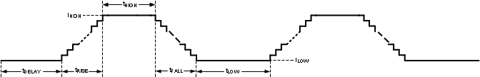 Figure 22. Pattern Generator Timing
Table 27. Control C to Control H Pattern Generator Delay Time (Address 0x50, 0x60, 0x70, 0x80, 0x90, 0xA0)
| Bit [7] | Bits [6:0] tDELAY times |
|---|---|
| Reserved | 0x00 = 16.384 ms (16.384 ms/step) (default) |
| 0x01 = 32.768 ms | |
| : | |
| : | |
| 0x3B = 983.05 ms | |
| 0x3C = 999.424 ms | |
| 0x3D = 1130.496 ms (131.072 ms/step) | |
| 0x3E = 1261.568 ms | |
| : | |
| : | |
| 0x7F = 9781.248 ms |
Table 28. Control C to Control H Pattern Generator Low Time (Address 0x51, 0x61, 0x71, 0x81, 0x91, 0xA1)
| Bits [7:0] |
|---|
| tLOW times |
| 0x00 = 16.384 ms (16.384 ms/step) (default) |
| 0x01 = 32.768 ms |
| : |
| : |
| 0x3B = 983.05 ms |
| 0x3C = 999.424 ms |
| 0x3D = 1130.496 ms (131.072 ms/step) |
| 0x3E = 1261.568 ms |
| : |
| : |
| 0x7F = 9781.248 ms |
| 0x80 = 10.305536 s (524.288 ms/step) |
| : |
| : |
| 0xFF = 76.890112 s |
Table 29. Control C to Control H Pattern Generator High Time (Address 0x52, 0x62, 0x72, 0x82, 0x92, 0xA2)
| Bit [7] Not Used |
Bits [6:0] tHIGH times |
|---|---|
| 0x00 = 16.384 ms (16.384 ms/step) (default) | |
| 0x01 = 32.768 ms | |
| : | |
| : | |
| 0x3B = 983.05 ms | |
| 0x3C = 999.424 ms | |
| 0x3D = 1130.496 ms (131.072 ms/step) | |
| 0x3E = 1261.568 ms | |
| : | |
| : | |
| 0x7F = 9781.248 ms |
Table 30. Control C to Control H Pattern Generator Low-Level Brightness (Address 0x53, 0x63, 0x73, 0x83, 0x93, 0xA3)
| Bits [7:0] Controls C to H Low-Level Brightness (BREGL_X) |
|---|
| Brightness Code (refer to Low-Level Brightness) |
Table 31. HVLED Open Faults (Address 0xB0)
| Bits [7:3] Not Used |
Bit [2] HVLED3 Open |
Bit [1] HVLED2 Open |
Bit [0] HVLED1 Open |
|---|---|---|---|
| Reserved | 0 = Normal Operation 1 = Open |
0 = Normal Operation 1 = Open |
0 = Normal Operation 1 = Open |
Table 32. LVLED Open Faults (Address 0xB1)
| Bits [7:6] Not Used |
Bit [5] LVLED6 Open |
Bit [4] LVLED5 Open |
Bit [3] LVLED4 Open |
Bit [2] LVLED3 Open |
Bit [1] LVLED2 Open |
Bit [0] LVLED1 Open |
|---|---|---|---|---|---|---|
| Reserved | 0 = Normal Operation 1 = Open |
0 = Normal Operation 1 = Open |
0 = Normal Operation 1 = Open |
0 = Normal Operation 1 = Open |
0 = Normal Operation 1 = Open |
0 = Normal Operation 1 = Open |
Table 33. HVLED Short Faults (Address 0xB2)
| Bits [7:3] Not Used |
Bit [2] HVLED3 Short |
Bit [1] HVLED2 Short |
Bit [0] HVLED1 Short |
|---|---|---|---|
| Reserved | 0 = Normal Operation 1 = Short |
0 = Normal Operation 1 = Short |
0 = Normal Operation 1 = Short |
Table 34. LVLED Short Faults (Address 0xB3)
| Bits [7:6] Not Used |
Bit [5] LVLED6 Short |
Bit [4] LVLED5 Short |
Bit [3] LVLED4 Short |
Bit [2] LVLED3 Short |
Bit [1] LHVLED2 Short |
Bit [0] LVLED1 Short |
|---|---|---|---|---|---|---|
| Reserved | 0 = Normal Operation 1 = Short |
0 = Normal Operation 1 = Short |
0 = Normal Operation 1 = Short |
0 = Normal Operation 1 = Short |
0 = Normal Operation 1 = Short |
0 = Normal Operation 1 = Short |
Table 35. LED Fault Enable (Address 0xB4)
| Bits [7:2] Not Used |
Bit [1] Short Faults Enable |
Bit [0] Open Faults Enable |
|---|---|---|
| Reserved | 0 = Disable (default) 1 = Enable |
0 = Disable (default) 1 = Enable |