SNVSA68D October 2014 – November 2016 LM3648
PRODUCTION DATA.
- 1 Features
- 2 Applications
- 3 Description
- 4 Revision History
- 5 Pin Configuration and Functions
- 6 Specifications
-
7 Detailed Description
- 7.1 Overview
- 7.2 Functional Block Diagram
- 7.3 Feature Description
- 7.4 Device Functioning Modes
- 7.5 Programming
- 7.6
Register Descriptions
- 7.6.1 Enable Register (0x01)
- 7.6.2 IVFM Register (0x02)
- 7.6.3 LED Flash Brightness Register (0x03)
- 7.6.4 LED Torch Brightness Register (0x05)
- 7.6.5 Boost Configuration Register (0x07)
- 7.6.6 Timing Configuration Register (0x08)
- 7.6.7 TEMP Register (0x09)
- 7.6.8 Flags1 Register (0x0A)
- 7.6.9 Flags2 Register (0x0B)
- 7.6.10 Device ID Register (0x0C)
- 7.6.11 Last Flash Register (0x0D)
- 8 Applications and Implementation
- 9 Power Supply Recommendations
- 10Layout
- 11Device and Documentation Support
- 12Mechanical, Packaging, and Orderable Information
Package Options
Mechanical Data (Package|Pins)
- YFF|12
Thermal pad, mechanical data (Package|Pins)
Orderable Information
6 Specifications
6.1 Absolute Maximum Ratings
over operating free-air temperature range (unless otherwise noted)(1)(2)| MIN | MAX | UNIT | ||
|---|---|---|---|---|
| IN, SW, OUT, LED | −0.3 | 6 | V | |
| SDA, SCL, TX, TORCH/TEMP, HWEN, STROBE | −0.3 | (VIN+ 0.3) w/ 6 V max | ||
| Continuous power dissipation(3) | Internally limited | |||
| Junction temperature (TJ-MAX) | 150 | °C | ||
| Maximum lead temperature (soldering) | See(4) | |||
| Storage temperature, Tstg | −65 | 150 | °C | |
(1) Stresses beyond those listed under Absolute Maximum Ratings may cause permanent damage to the device. These are stress ratings only, which do not imply functional operation of the device at these or any other conditions beyond those indicated under Recommended Operating Conditions. Exposure to absolute-maximum-rated conditions for extended periods may affect device reliability.
(2) All voltages are with respect to the potential at the GND pin.
(3) Internal thermal shutdown circuitry protects the device from permanent damage. Thermal shutdown engages at TJ = 150°C (typical) and disengages at TJ = 135°C (typical). Thermal shutdown is ensured by design.
(4) For detailed soldering specifications and information, refer to Texas Instruments Application Note 1112: DSBGA Wafer Level Chip Scale Package (SNVA009).
6.2 ESD Ratings
| VALUE | UNIT | |||
|---|---|---|---|---|
| V(ESD) | Electrostatic discharge | Human-body model (HBM), per ANSI/ESDA/JEDEC JS-001(1) | ±2500 | V |
| Charged-device model (CDM), per JEDEC specification JESD22-C101(2) | ±150 | |||
(1) JEDEC document JEP155 states that 500-V HBM allows safe manufacturing with a standard ESD control process.
(2) JEDEC document JEP157 states that 250-V CDM allows safe manufacturing with a standard ESD control process.
6.3 Recommended Operating Conditions
over operating free-air temperature range (unless otherwise noted)(1)(2)| MIN | MAX | UNIT | ||
|---|---|---|---|---|
| VIN | 2.5 | 5.5 | V | |
| Junction temperature (TJ) | −40 | 125 | °C | |
| Ambient temperature (TA) (3) | −40 | 85 | °C | |
(1) Stresses beyond those listed under absolute maximum ratings may cause permanent damage to the device. These are stress ratings only, and functional operation of the device at these or any other conditions beyond those indicated under recommended operating conditions is not implied. Exposure to absolute-maximum-rated conditions for extended periods may affect device reliability.
(2) All voltages are with respect to the potential at the GND terminal.
(3) In applications where high power dissipation and/or poor package thermal resistance is present, the maximum ambient temperature may have to be derated. Maximum ambient temperature (TA-MAX) is dependent on the maximum operating junction temperature (TJ-MAX-OP = 125°C), the maximum power dissipation of the device in the application (PD-MAX), and the junction-to-ambient thermal resistance of the part/package in the application (RθJA), as given by the following equation: TA-MAX = TJ-MAX-OP – (RθJA × PD-MAX).
6.4 Thermal Information
| THERMAL METRIC(1) | LM3648 | UNIT | |
|---|---|---|---|
| YFF (DSBGA) | |||
| 12 PINS | |||
| RθJA | Junction-to-ambient thermal resistance | 90.2 | °C/W |
| RθJC(top) | Junction-to-case (top) thermal resistance | 0.5 | °C/W |
| RθJB | Junction-to-board thermal resistance | 40.0 | °C/W |
| ΨJT | Junction-to-top characterization parameter | 3.0 | °C/W |
| ΨJB | Junction-to-board characterization parameter | 39.2 | °C/W |
(1) For more information about traditional and new thermal metrics, see the Semiconductor and IC Package Thermal Metrics.
6.5 Electrical Characteristics
Typical limits tested at TA = 25°C. Minimum and maximum limits apply over the full operating ambient temperature range (−40°C ≤ TA ≤ +85°C). Unless otherwise specified, VIN = 3.6 V, HWEN = VIN.(1)(2)
(1) Minimum (MIN) and Maximum (MAX) limits are specified by design, test, or statistical analysis. Typical (TYP) numbers are not verified, but do represent the most likely norm. Unless otherwise specified, conditions for typical specifications are: VIN = 3.6 V and TA = 25°C.
(2) All voltages are with respect to the potential at the GND pin.
6.6 Timing Requirements
6.7 Switching Characteristics
over operating free-air temperature range (unless otherwise noted)| PARAMETER | TEST CONDITIONS | MIN | TYP | MAX | UNIT | |
|---|---|---|---|---|---|---|
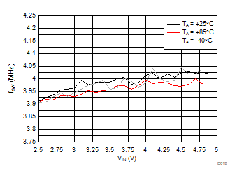
| ƒSW | Switching frequency | 2.5 V ≤ VIN ≤ 5.5 V | –6% | 4 | 6% | MHz |
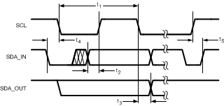 Figure 1. I2C-Compatible Interface Specifications
6.8 Typical Characteristics
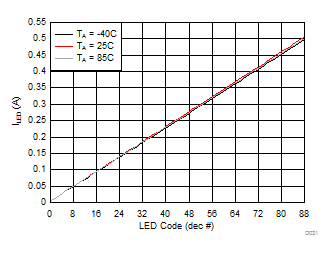
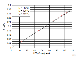
TA = 25°C, VIN = 3.6 V, HWEN = VIN, CIN = COUT = 2 × 10 µF and L = 1 µH, unless otherwise noted.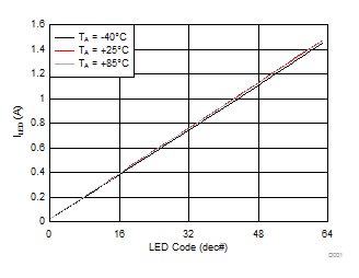
| LM3648TT | ||
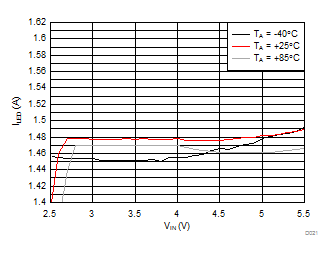
| ƒSW = 2 MHz | Flash | |
| Brightness Code = 0x3F | ||
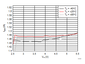
| ƒSW = 4 MHz | Flash | |
| Brightness Code = 0x3F | ||

| ƒSW = 2 MHz | Torch | |
| Brightness Code = 0x7F | ||
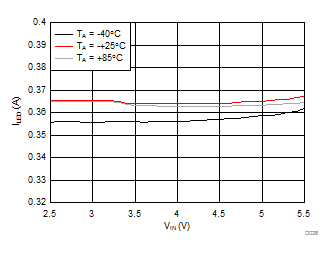
| ƒSW = 4 MHz | Torch | |
| Brightness Code = 0x7F | ||
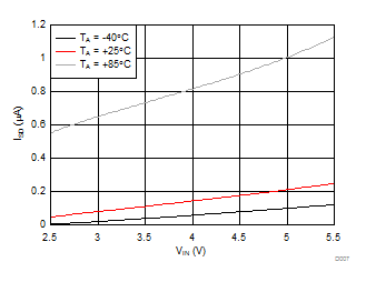
| HWEN = 0 V | I2C = 0 V | |

| HWEN = 1.8 V | I2C = 0 V | |
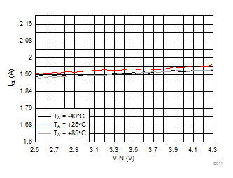
| ƒSW = 2 MHz | Flash | VLED = 4.5 V |
| Brightness Code = 0x3F | ICL = 1.9 A | |
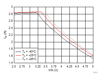
| ƒSW = 2 MHz | Flash | VLED = 4.5 V |
| Brightness Code = 0x3F | ICL = 2.8 A | |
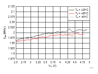
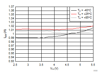
| ƒSW = 2 MHz | Flash | |
| Brightness Code = 0x2B | ||
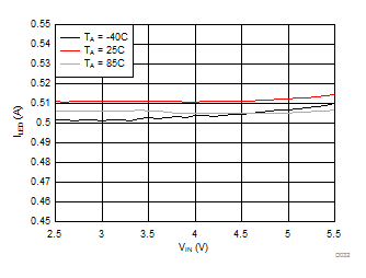
| LM3648TT | ƒSW = 2 MHz | Torch |
| Brightness Code = 0x59 | ||
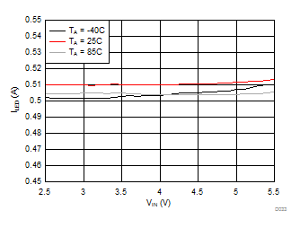
| LM3648TT | ƒSW = 4 MHz | Torch |
| Brightness Code = 0x59 | ||
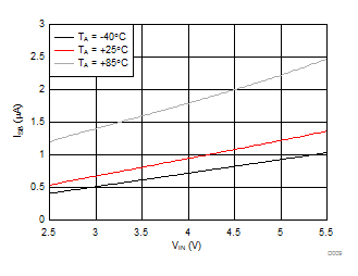
| HWEN = VIN | I2C = VIN | |
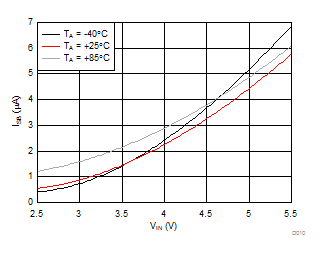
| HWEN = 1.8 V | I2C = 1.8 V | |
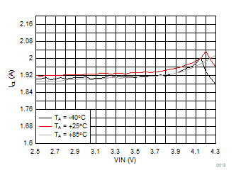
| ƒSW = 4 MHz | Flash | VLED = 4.5 V |
| Brightness Code = 0x3F | ICL = 1.9 A | |
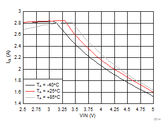
| ƒSW = 4 MHz | Flash | VLED = 4.5 V |
| Brightness Code = 0x3F | ICL = 2.8 A | |
