SNVS506J May 2008 – December 2015 LM3691
PRODUCTION DATA.
- 1 Features
- 2 Applications
- 3 Description
- 4 Revision History
- 5 Voltage Options
- 6 Pin Configuration and Functions
- 7 Specifications
- 8 Detailed Description
- 9 Application and Implementation
- 10Power Supply Recommendations
- 11Layout
- 12Device and Documentation Support
- 13Mechanical, Packaging, and Orderable Information
Package Options
Mechanical Data (Package|Pins)
- YZR|6
Thermal pad, mechanical data (Package|Pins)
Orderable Information
1 Features
- Input Voltage: 2.3 V to 5.5 V
- Output Voltage: 0.75 V to 3.3 V
- ±1% DC Output Voltage Precision
- 4-MHz Switching Frequency
- 64-μA (typical) Quiescent Current in ECO Mode
- 1-A Maximum Load Capability
- Automatic ECO/PWM Mode Switching
- MODE Pin to Select ECO/Forced PWM Mode
- Current Overload and Thermal Shutdown Protections
- Only Three Tiny Surface-Mount External Components Required (Solution Size Less Than 15 mm2)
2 Applications
- Mobile Phones
- Hand-Held Radios
- MP3 Players
- Portable Hard Disk Drives
3 Description
The LM3691 step-down DC-DC converter is optimized for powering ultra-low-voltage circuits from a single Li-Ion cell or 3 cell NiMH/NiCd batteries. It provides up to 1-A load current over an input voltage range from 2.3 V to 5.5 V. There are several different fixed voltage output options available.
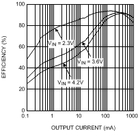
The LM3691 has a mode-control pin that allows the user to select Forced PWM mode or ECO mode that changes modes between gated PWM mode and PWM automatically, depending on the load. In ECO mode, the device offers superior efficiency and very low IQ under light load conditions. ECO mode extends the battery life through reduction of the quiescent current during light load conditions and system standby.
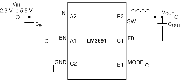
The LM3691 is available in a 6-pin DSBGA package. Only three external surface-mount components, a
1-μH inductor, a 4.7-μF input capacitor, and a 4.7-μF output capacitor, are required.
Device Information(1)
| PART NUMBER | PACKAGE | BODY SIZE (MAX) |
|---|---|---|
| LM3691 | DSBGA (6) | 1.59 mm × 1.295 mm |
Typical Application Circuit

Efficiency vs. Output Current
(VOUT = 1.8 V, ECO Mode)
