SNVS506J May 2008 – December 2015 LM3691
PRODUCTION DATA.
- 1 Features
- 2 Applications
- 3 Description
- 4 Revision History
- 5 Voltage Options
- 6 Pin Configuration and Functions
- 7 Specifications
- 8 Detailed Description
- 9 Application and Implementation
- 10Power Supply Recommendations
- 11Layout
- 12Device and Documentation Support
- 13Mechanical, Packaging, and Orderable Information
Package Options
Mechanical Data (Package|Pins)
- YZR|6
Thermal pad, mechanical data (Package|Pins)
Orderable Information
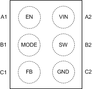
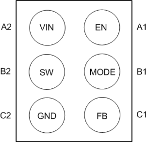
6 Pin Configuration and Functions
YZR Package
6-Pin DSBGA
Top View

YZR Package
6-Pin DSBGA
Bottom View

Pin Functions
| PIN | TYPE(1) | DESCRIPTION | ||
|---|---|---|---|---|
| NO. | NAME | |||
| A1 | EN | I | EN pin. The device is in shutdown mode when voltage to this pin is < 0.4 V and enabled when > 1.2 V. Do not leave this pin floating |
|
| A2 | VIN | P | Power supply input. Connect to the input filter capacitor. (See Typical Application Circuit.) | |
| B1 | MODE | I | MODE pin: Mode = 1, forced PWM; mode = 0, ECO Do not leave this pin floating. |
|
| B2 | SW | A | Switching node connection to the internal PFET switch and NFET synchronous rectifier. | |
| C1 | FB | A | Feedback analog input. Connect directly to the output filter capacitor. (See Typical Application Circuit.) |
|
| C2 | GND | G | Ground pin. | |
(1) A: Analog Pin, D: Digital Pin, G: Ground Pin, P: Power Pin, I: Input Pin, I/O; Input/Output, O: Output Pin