SNVS821A January 2014 – March 2014 LM3699
PRODUCTION DATA.
- 1 Features
- 2 Applications
- 3 Description
- 4 Revision History
- 5 Terminal Configuration and Functions
- 6 Specifications
- 7 Detailed Description
- 8 Application and Implementation
- 9 Power Supply Recommendations
- 10Layout
- 11Device and Documentation Support
- 12Mechanical, Packaging, and Orderable Information
Package Options
Mechanical Data (Package|Pins)
- YFQ|12
Thermal pad, mechanical data (Package|Pins)
Orderable Information
5 Terminal Configuration and Functions
DSBGA (YFQ)
12 Terminals
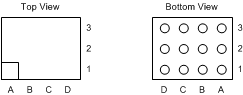
Terminal Functions
| TERMINAL | DESCRIPTION | |
|---|---|---|
| NUMBER | NAME | |
| A1 | PWM | PWM brightness control input. PWM is a high-impedance input and cannot be left floating. |
| A2 | IS0 | Current select input 1. This is a high-impedance input and cannot be left floating. IS0 can be connected to IN or GND. |
| A3 | HWEN | Hardware enable input. Drive this terminal high to enable the device. Drive this terminal low to force the device into a low-power shutdown. HWEN is a high-impedance input and cannot be left floating. |
| B1 | HVLED1 | Input terminal to high-voltage current sink 1 (24 V max). The boost converter regulates the minimum of HVLED1, HVLED2, and HVLED3 to VHR. |
| B2 | IS1 | Current select input 2. This is a high-impedance input and cannot be left floating. IS1 can be connected to IN or GND. |
| B3 | IN | Input voltage connection. Bypass IN to GND with a minimum 2.2-µF ceramic capacitor. |
| C1 | HVLED2 | Input terminal to high-voltage current sink 2 (24 V max). The boost converter regulates the minimum of HVLED1, HVLED2, and HVLED3 to VHR. |
| C2 | ILOW | Low level current enable. Drive this terminal high to reduce LED current by approximately 95%. ILOW is a high-impedance input and cannot be left floating. If not used connect to GND. |
| C3 | GND | Ground. |
| D1 | HVLED3 | Input terminal to high-voltage current sink 3 (24 V max). The boost converter regulates the minimum of HVLED1, HVLED2, and HVLED3 to VHR. |
| D2 | OVP | Overvoltage sense input. Connect OVP to the positive terminal of the inductive boost output capacitor (COUT). |
| D3 | SW | Drain connection for the internal NFET. Connect SW to the junction of the inductor and the Schottky diode anode. |