SNVS053F June 2000 – September 2016 LM4140
PRODUCTION DATA.
- 1 Features
- 2 Applications
- 3 Description
- 4 Revision History
- 5 Pin Configuration and Functions
- 6 Specifications
- 7 Detailed Description
-
8 Application and Implementation
- 8.1 Application Information
- 8.2
Typical Applications
- 8.2.1 Precision DAC Reference
- 8.2.2 Boosted Output Current
- 8.2.3 Boosted Output Current With Current Limiter
- 8.2.4 Complimentary Outputs
- 8.2.5 Voltage Reference With Force and Sense Output
- 8.2.6 Precision Programmable Current Source
- 8.2.7 Strain Gauge Conditioner for 350-Ω Bridge
- 8.2.8 Bipolar Voltage References for Low Power ADC
- 8.2.9 Self-Biased Low Power ADC Reference With Trim Current Sources
- 9 Power Supply Recommendations
- 10Layout
- 11Device and Documentation Support
- 12Mechanical, Packaging, and Orderable Information
Package Options
Mechanical Data (Package|Pins)
- D|8
Thermal pad, mechanical data (Package|Pins)
Orderable Information
6 Specifications
6.1 Absolute Maximum Ratings
over operating free-air temperature range (unless otherwise noted)(1)| MIN | MAX | UNIT | ||
|---|---|---|---|---|
| Maximum voltage on any input pin | –0.3 | 5.6 | V | |
| Output short-circuit duration | Indefinite | |||
| Power dissipation (TA = 25°C)(2) | 345 | mW | ||
| Storage temperature, Tstg | –65 | 150 | °C | |
(1) Stresses beyond those listed under Absolute Maximum Ratings may cause permanent damage to the device. These are stress ratings only, which do not imply functional operation of the device at these or any other conditions beyond those indicated under Recommended Operating Conditions. Exposure to absolute-maximum-rated conditions for extended periods may affect device reliability.
(2) Without PCB copper enhancements. The maximum power dissipation must be derated at elevated temperatures and is limited by TJMAX (maximum junction temperature), RθJA (junction to ambient thermal resistance) and TA (ambient temperature). The maximum power dissipation at any temperature is: PDissMAX = (TJMAX − TA)/RθJA up to the value listed in the Absolute Maximum Ratings. The RθJA for the 8-pin SOIC package is 160°C/W.
6.2 ESD Ratings
| VALUE | UNIT | |||
|---|---|---|---|---|
| V(ESD) | Electrostatic discharge | Human-body model (HBM), per ANSI/ESDA/JEDEC JS-001(1) | ±2000 | V |
| Charged-device model (CDM), per JEDEC specification JESD22-C101(2) | ±200 | |||
(1) JEDEC document JEP155 states that 500-V HBM allows safe manufacturing with a standard ESD control process.
(2) JEDEC document JEP157 states that 250-V CDM allows safe manufacturing with a standard ESD control process.
6.3 Recommended Operating Conditions
over operating free-air temperature range (unless otherwise noted)| MIN | NOM | MAX | UNIT | |
|---|---|---|---|---|
| Ambient temperature | 0 | 70 | °C | |
| Junction temperature | 0 | 80 | °C |
6.4 Thermal Information
| THERMAL METRIC(1) | LM4140 | UNIT | |
|---|---|---|---|
| D (SOIC) | |||
| 8 PINS | |||
| RθJA | Junction-to-ambient thermal resistance | 119.3 | °C/W |
| RθJC(top) | Junction-to-case (top) thermal resistance | 52.3 | °C/W |
| RθJB | Junction-to-board thermal resistance | 60.3 | °C/W |
| ψJT | Junction-to-top characterization parameter | 14.5 | °C/W |
| ψJB | Junction-to-board characterization parameter | 59.7 | °C/W |
| RθJC(bot) | Junction-to-case (bottom) thermal resistance | — | °C/W |
(1) For more information about traditional and new thermal metrics, see the Semiconductor and IC Package Thermal Metrics application report.
6.5 Electrical Characteristics
VIN = 3 V for the 1.024-V and 1.25-V, VIN = 5 V for all other voltage options, VEN = VIN, COUT = 1 µF(1), ILOAD = 1 mA, andTA = TJ = 25°C (unless otherwise noted)
| PARAMETER | TEST CONDITIONS | MIN(2) | TYP(3) | MAX(2) | UNIT | |||
|---|---|---|---|---|---|---|---|---|
| VREF | Output voltage initial accuracy(4) | All versions | ±0.1% | |||||
| TCVREF/°C | Temperature coefficient | 0°C ≤ TA ≤ 70°C | A grade | 3 | ppm/°C | |||
| B grade | 6 | |||||||
| C grade | 10 | |||||||
| ΔVREF/ΔVIN | Line regulation | 1.024-V and 1.25-V options, 1.8 V ≤ VIN ≤ 5.5 V | TA = 25°C | 50 | 300 | ppm/V | ||
| 0°C ≤ TA ≤ 70°C | 350 | |||||||
| All other voltage options, Vref + 200 mV ≤ VIN ≤ 5.5 V |
TA = 25°C | 20 | 200 | |||||
| 0°C ≤ TA ≤ 70°C | 250 | |||||||
| ΔVREF/ΔILOAD | Load regulation | 1 mA ≤ ILOAD ≤ 8 mA | All other voltage options | TA = 25°C | 1 | 20 | ppm/mA | |
| 0°C ≤ TA ≤ 70°C | 150 | |||||||
| 4.096-V option | TA = 25°C | 5 | 35 | |||||
| 0°C ≤ TA ≤ 70°C | 150 | |||||||
| ΔVREF | Long-term stability | 1000 hours | 60 | ppm | ||||
| ΔVREF | Thermal hysteresis(5) | 0°C ≤ TA ≤ + 70°C | 20 | ppm | ||||
| Operating voltage | 1.024-V and 1.25-V options, IL = 1 mA to 8 mA, 0°C ≤ TA ≤ 70°C | 1.8 | 5.5 | V | ||||
| VIN-VREF | Dropout voltage(6) | 2.048-V and 2.5-V options | IL = 1 mA | TA = 25°C | 20 | 40 | mV | |
| 0°C ≤ TA ≤ 70°C | 45 | |||||||
| IL = 8 mA | TA = 25°C | 160 | 235 | |||||
| 0°C ≤ TA ≤ 70°C | 400 | |||||||
| 4.096-V option | IL = 1 mA | TA = 25°C | 20 | 40 | ||||
| 0°C ≤ TA ≤ 70°C | 45 | |||||||
| IL = 8 mA | TA = 25°C | 195 | 270 | |||||
| 0°C ≤ TA ≤ 70°C | 490 | |||||||
| VN | Output noise voltage(7) | 0.1 Hz to 10 Hz | 2.2 | µVPP | ||||
| IS(ON) | Supply current | ILOAD = 0 mA | All other voltage options | TA = 25°C | 230 | 320 | µA | |
| 0°C ≤ TA ≤ 70°C | 375 | |||||||
| 4.096-V option | TA = 25°C | 265 | 350 | |||||
| 0°C ≤ TA ≤ 70°C | 400 | |||||||
| IS(OFF) | Supply current | VEnable < 0.4 V | TA = 25°C | 0.01 | µA | |||
| 0°C ≤ TA ≤ 70°C | 1 | |||||||
| VH | Logic high input voltage | 0°C ≤ TA ≤ 70°C | 0.8 × VIN | V | ||||
| IH | Logic high input current | 2 | nA | |||||
| VL | Logic low input voltage | 0°C ≤ TA ≤ 70°C | 0.4 | V | ||||
| IL | Logic low input current | 1 | nA | |||||
| ISC | Short-circuit current | TA = 25°C | 8.5 | 20 | 35 | mA | ||
| 0°C ≤ TA ≤ 70°C | 40 | |||||||
(1) For proper operation, a 1-µF capacitor is required between the output pin and the GND pin of the device.
(2) Limits are 100% production tested at 25°C. Limits over the operating temperature range are ensured through correlation using Statistical Quality Control (SQC) methods. The limits are used to calculate TI's Average Outgoing Quality Level (AOQL).
(3) Typical numbers are at 25°C and represent the most likely parametric norm.
(4) High temperature and mechanical stress associated with PCB assembly can have significant impact on the initial accuracy of the LM4140 and may create significant shifts in VREF.
(5) Thermal hysteresis is defined as the changes in 25°C output voltage before and after the cycling of the device from 0°C to 70°C.
(6) Dropout voltage is defined as the minimum input to output differential voltage at which the output voltage drops by 0.5% below the value measured with VIN = 3 V for the 1.024-V and 1.25-V, VIN = 5 V for all other voltage options.
(7) The output noise is based on 1.024 V option. Output noise is linearly proportional to VREF.
6.6 Typical Characteristics
TA = 25°C, no load, COUT = 1 µF, VIN = 3 V for 1.024-V and 1.25-V, and 5 V for all other voltage options, and VIN = VEN (unless otherwise noted). The 1-µF output capacitor is actively discharged to ground (see ON/OFF Operation for more details).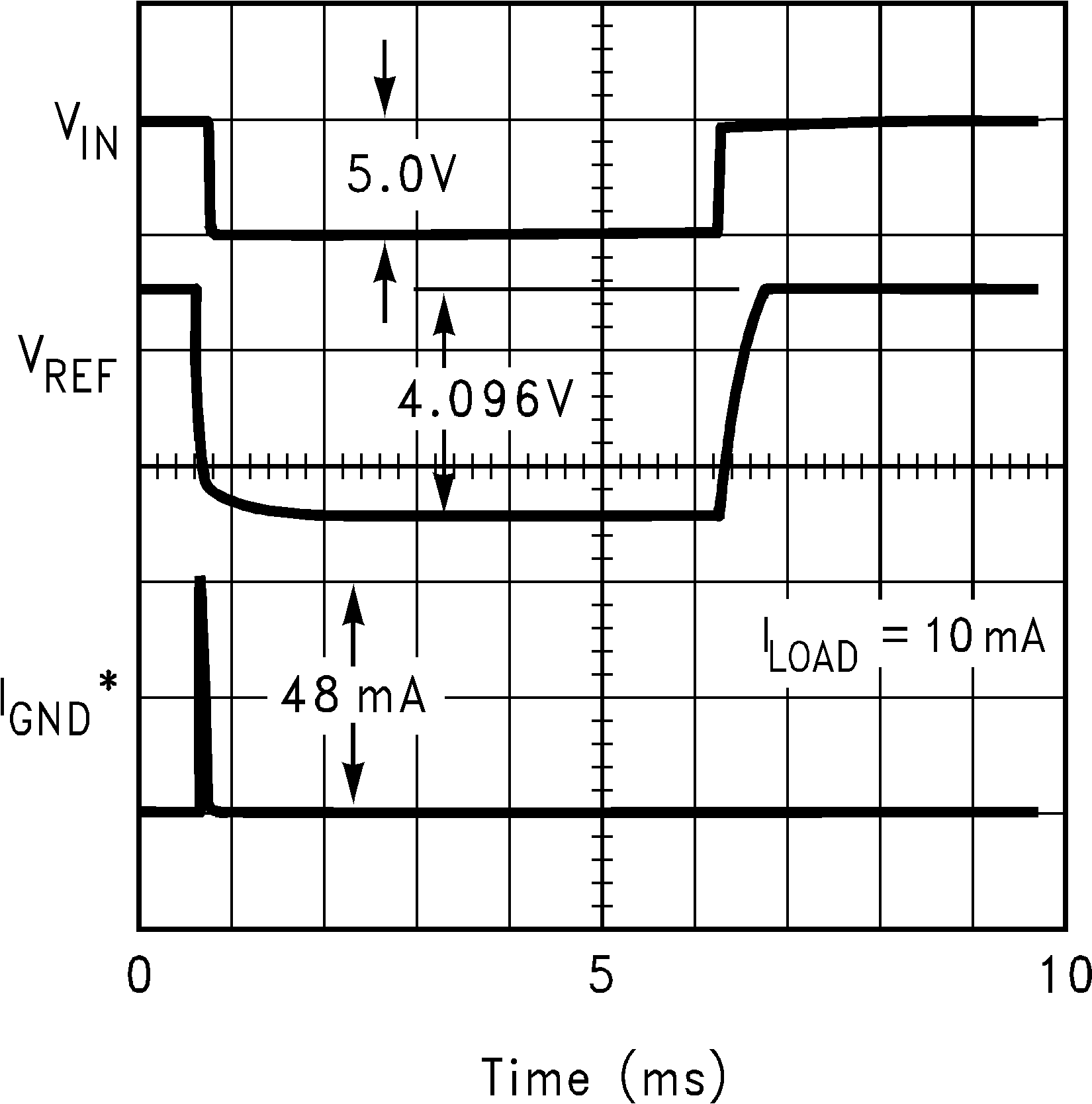 Figure 1. Power Up and Down Ground Current
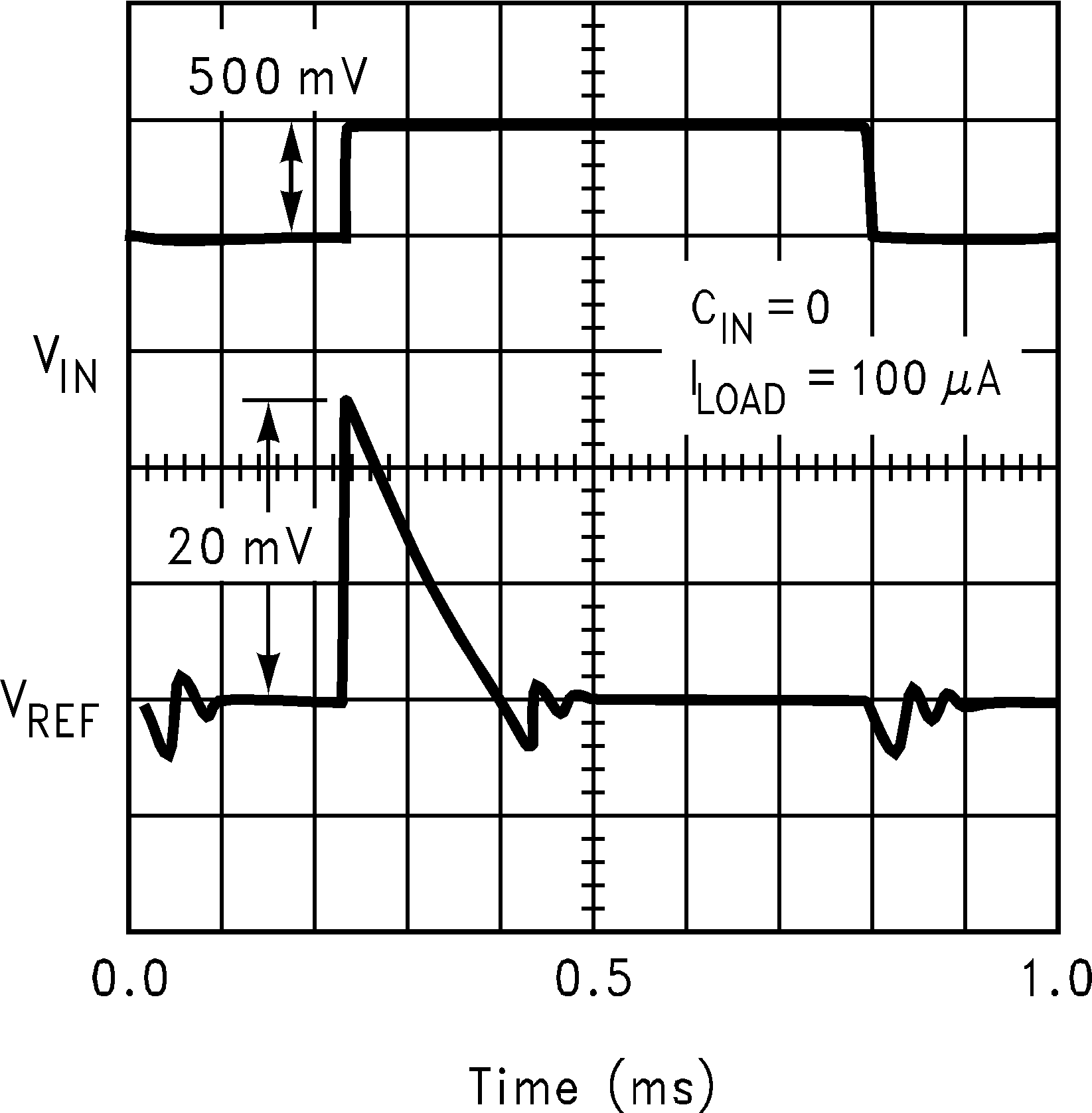 Figure 3. Line Transient Response
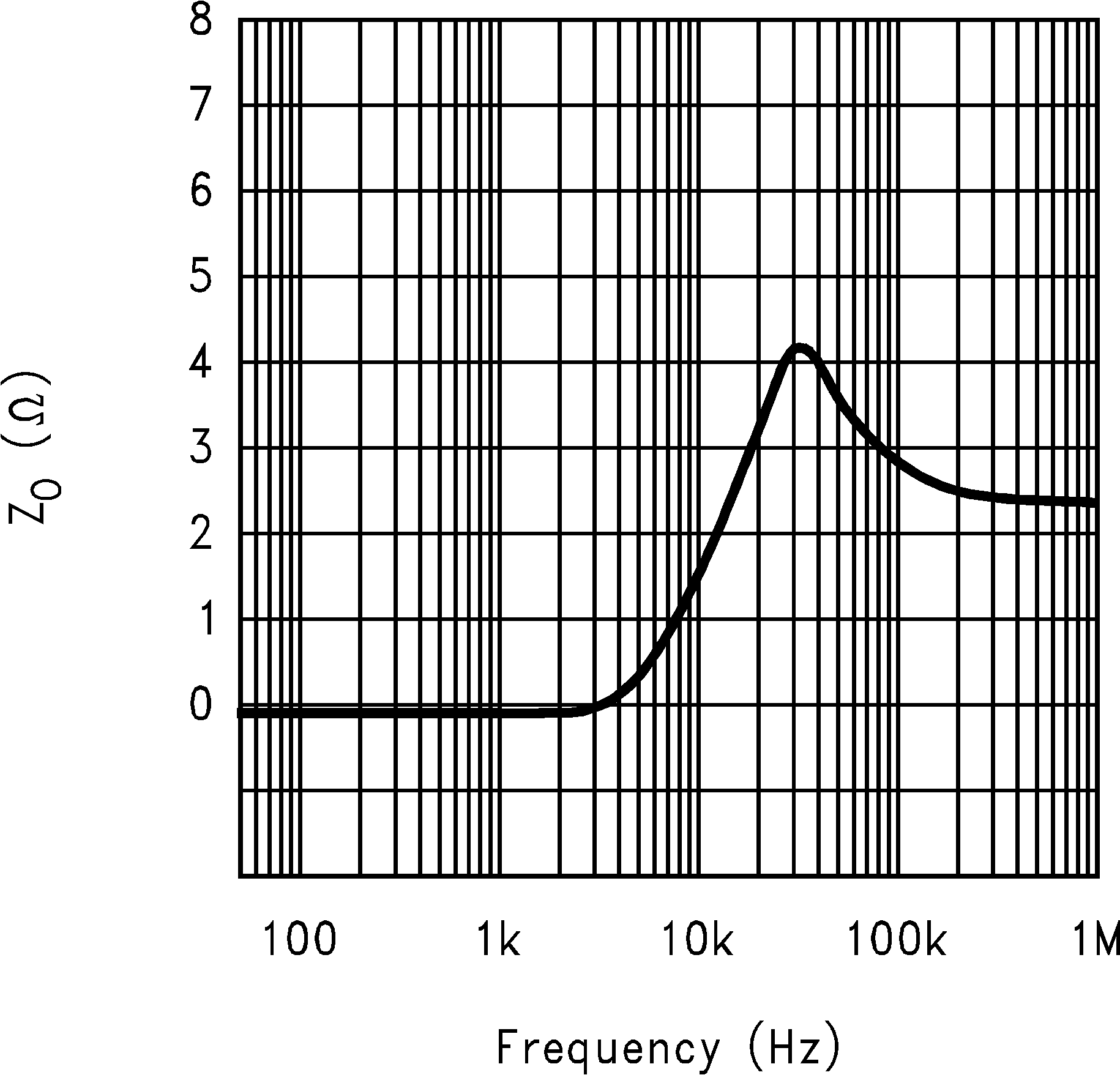 Figure 5. Output Impedance
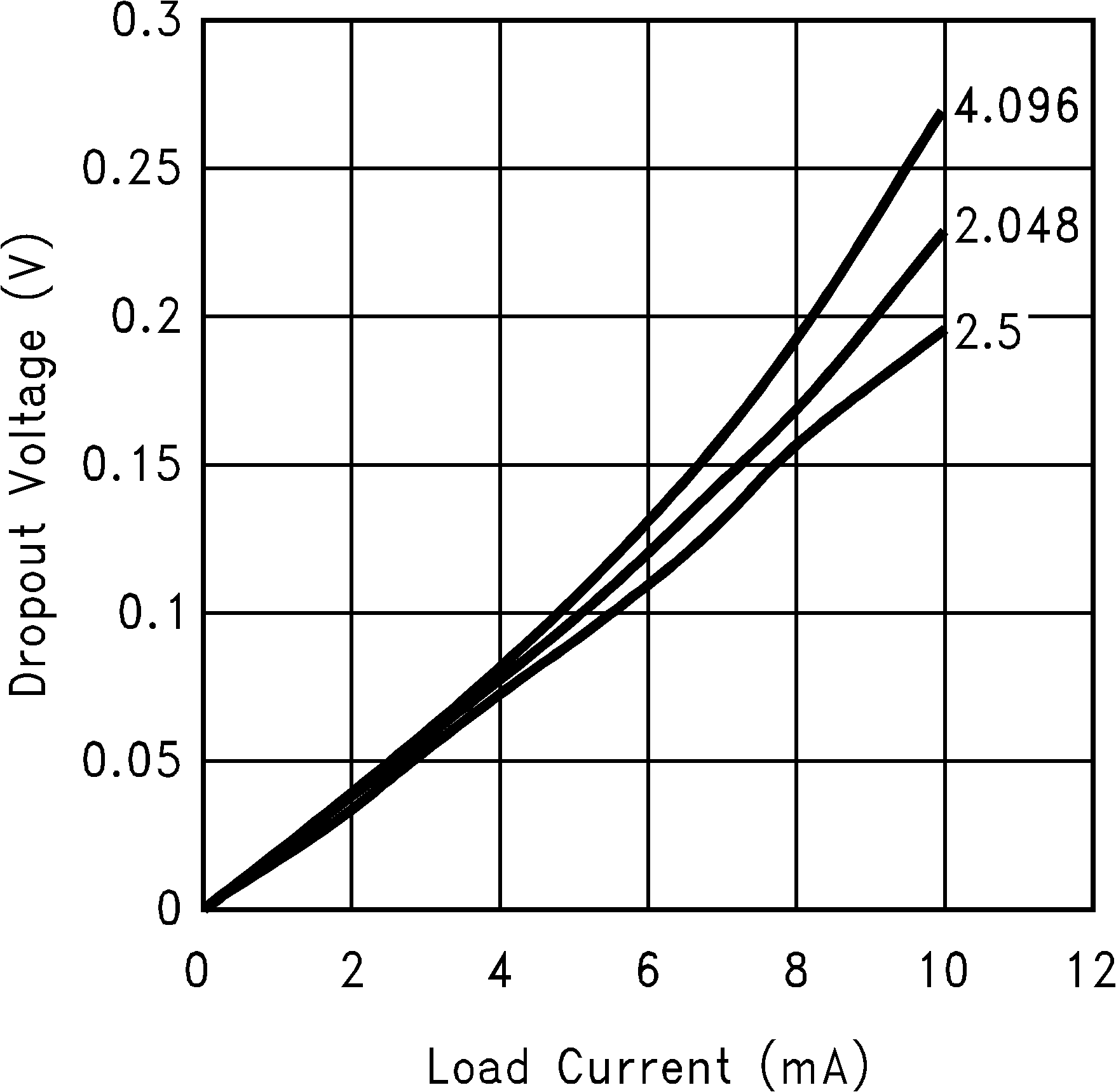
1.024-V and 1.25-V options require 1.8-V supply
Figure 7. Dropout Voltage vs Load Current
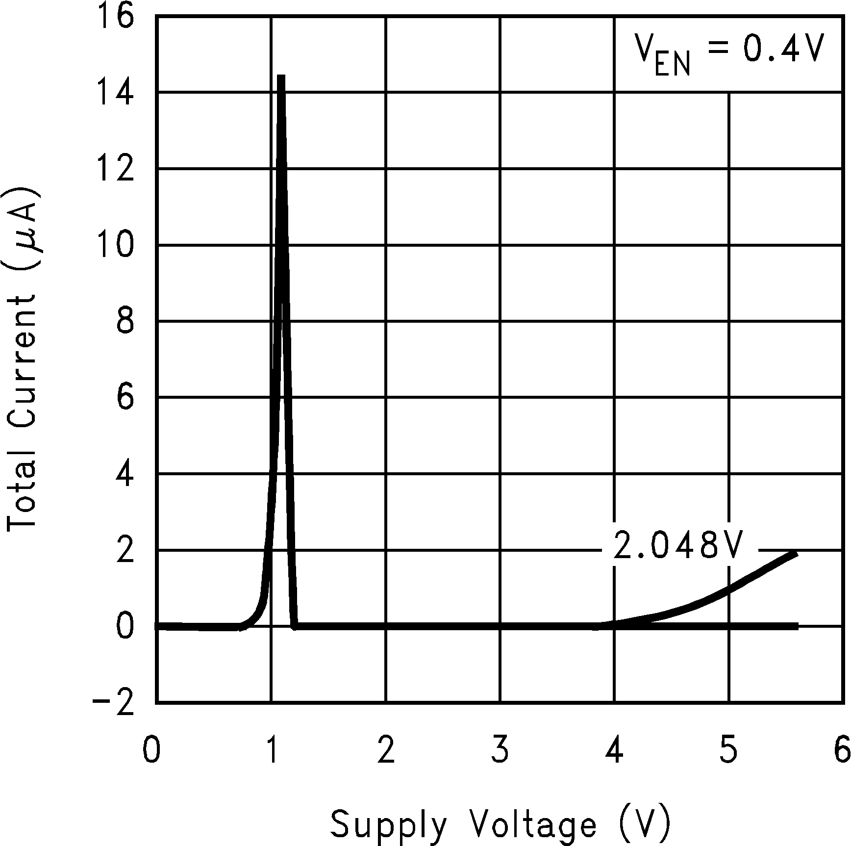 Figure 9. Total Current (IS(OFF)) vs Supply Voltage
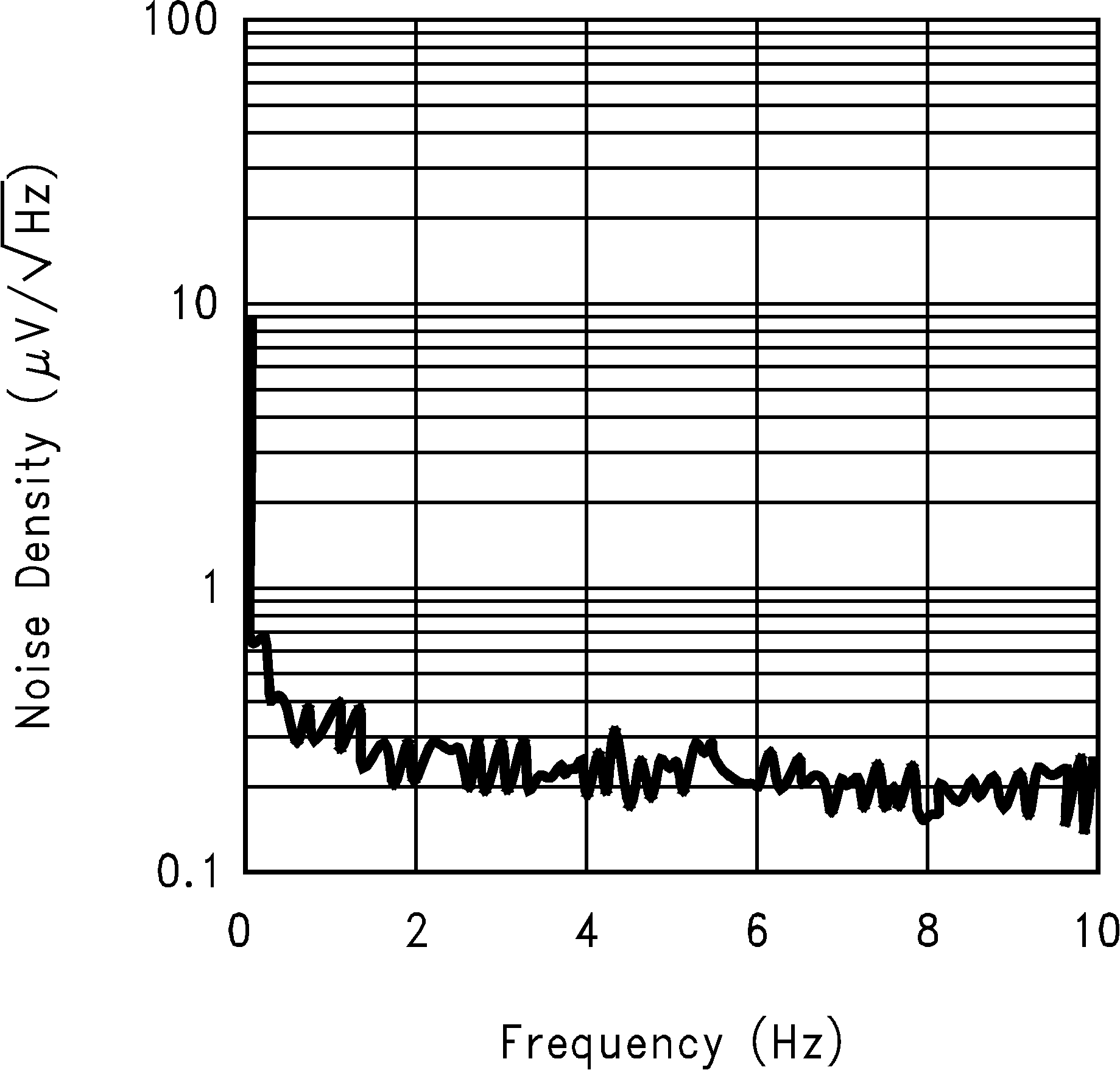 Figure 11. Spectral Noise Density (0.1 Hz to 10 Hz)
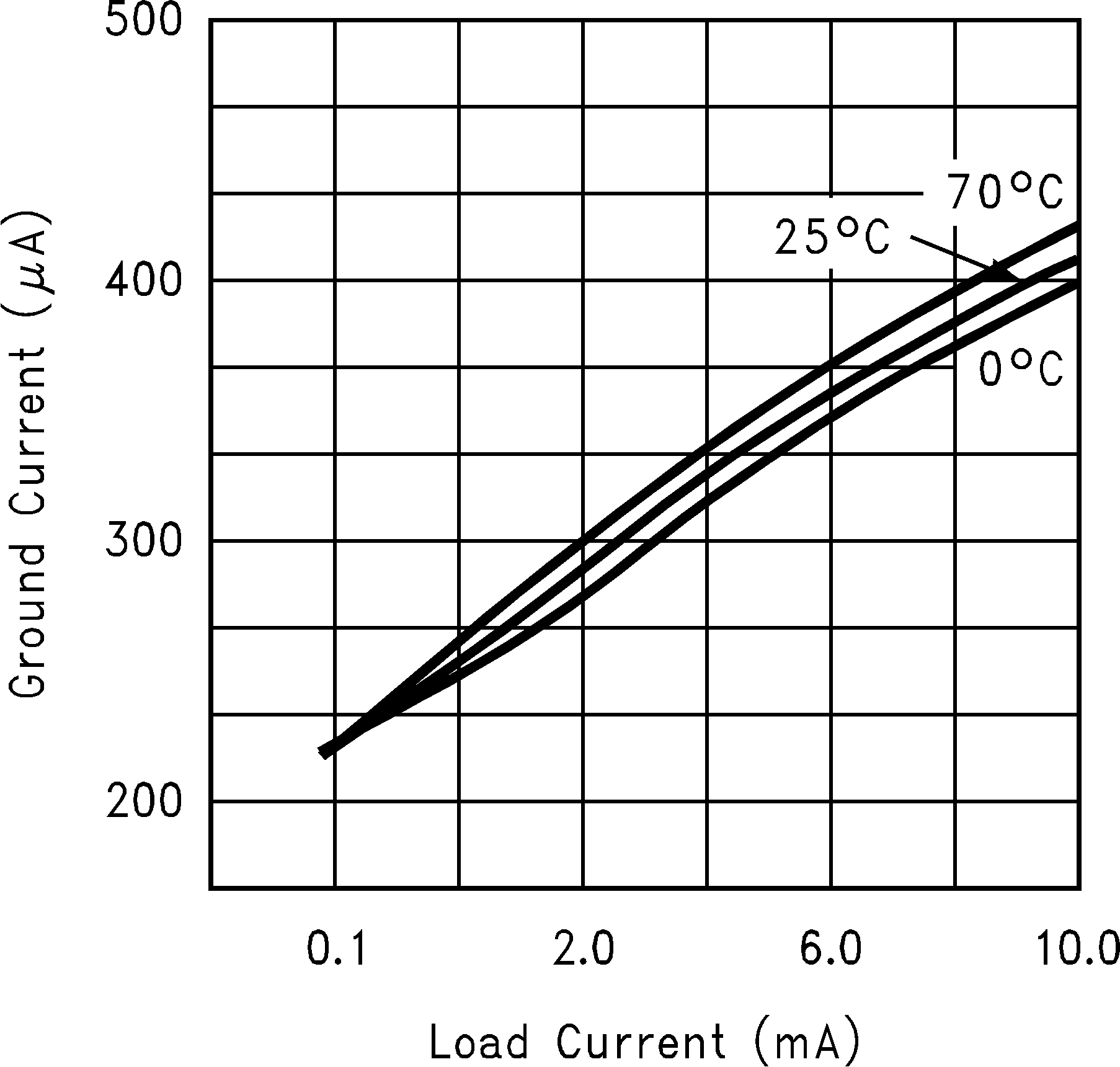 Figure 13. Ground Current vs Load Current
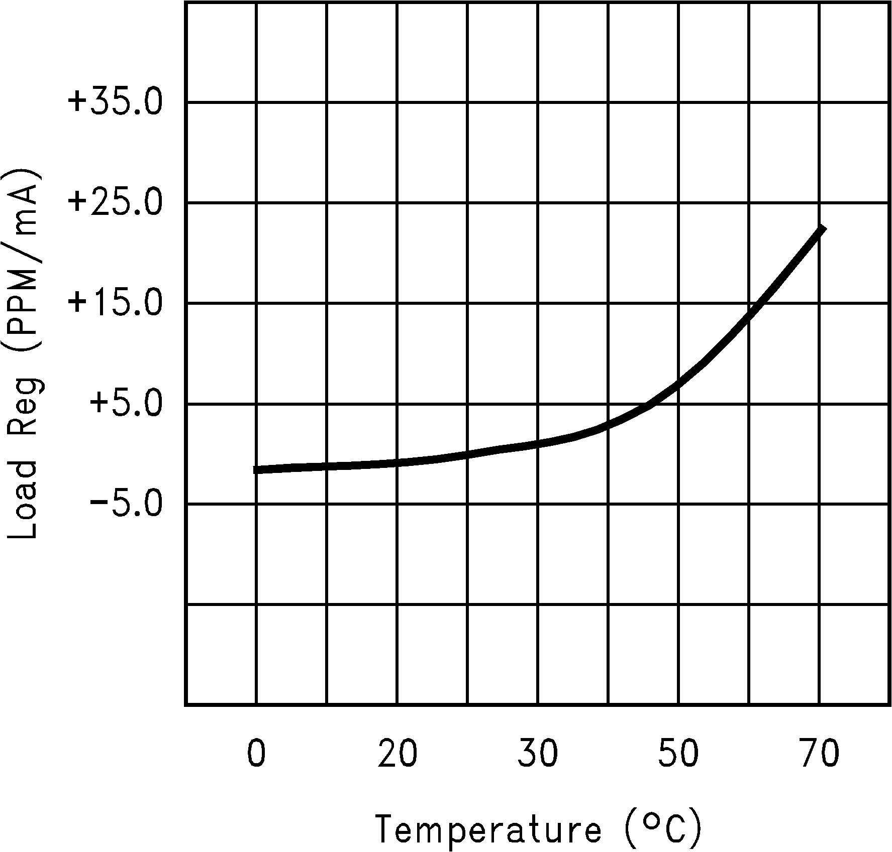 Figure 15. Load Regulation vs Temperature
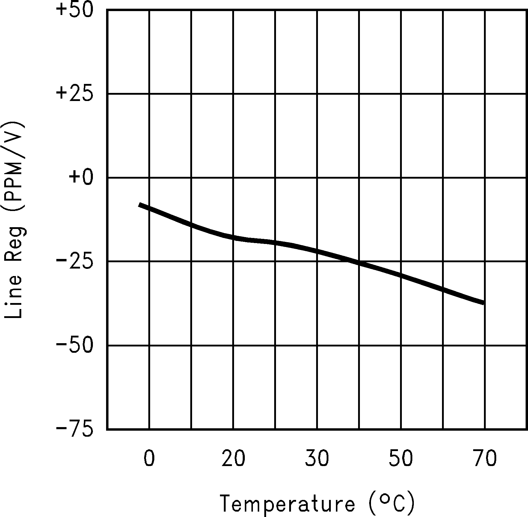 Figure 17. Line Regulation vs Temperature
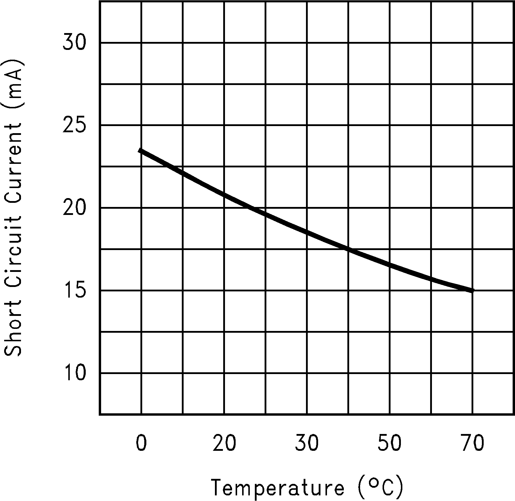 Figure 19. Short-Circuit Current vs Temperature
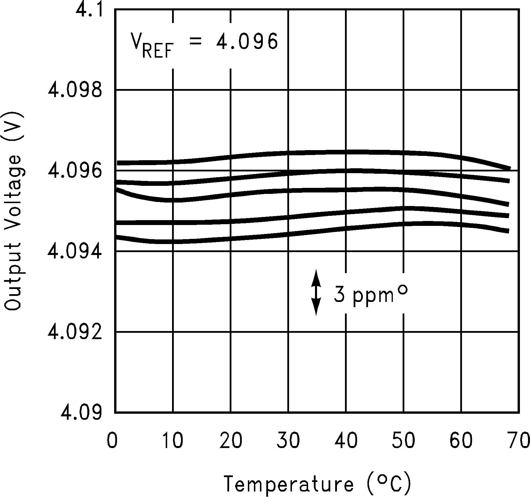 Figure 21. Typical Temperature Coefficient (Sample of 5 Parts)
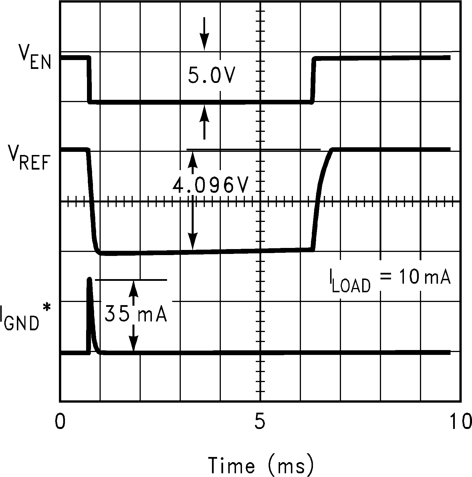 Figure 2. Enable Response
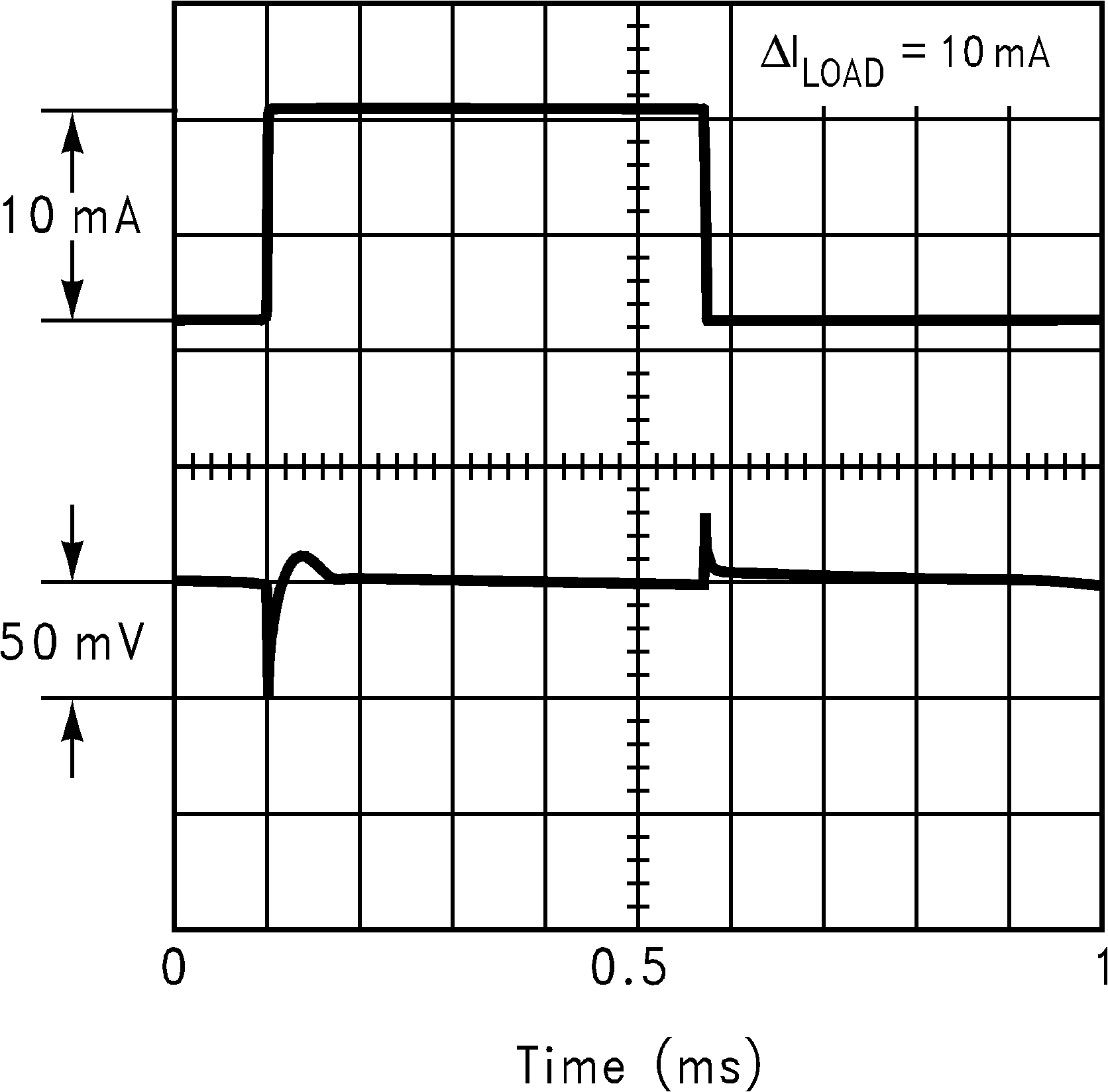 Figure 4. Load Transient Response
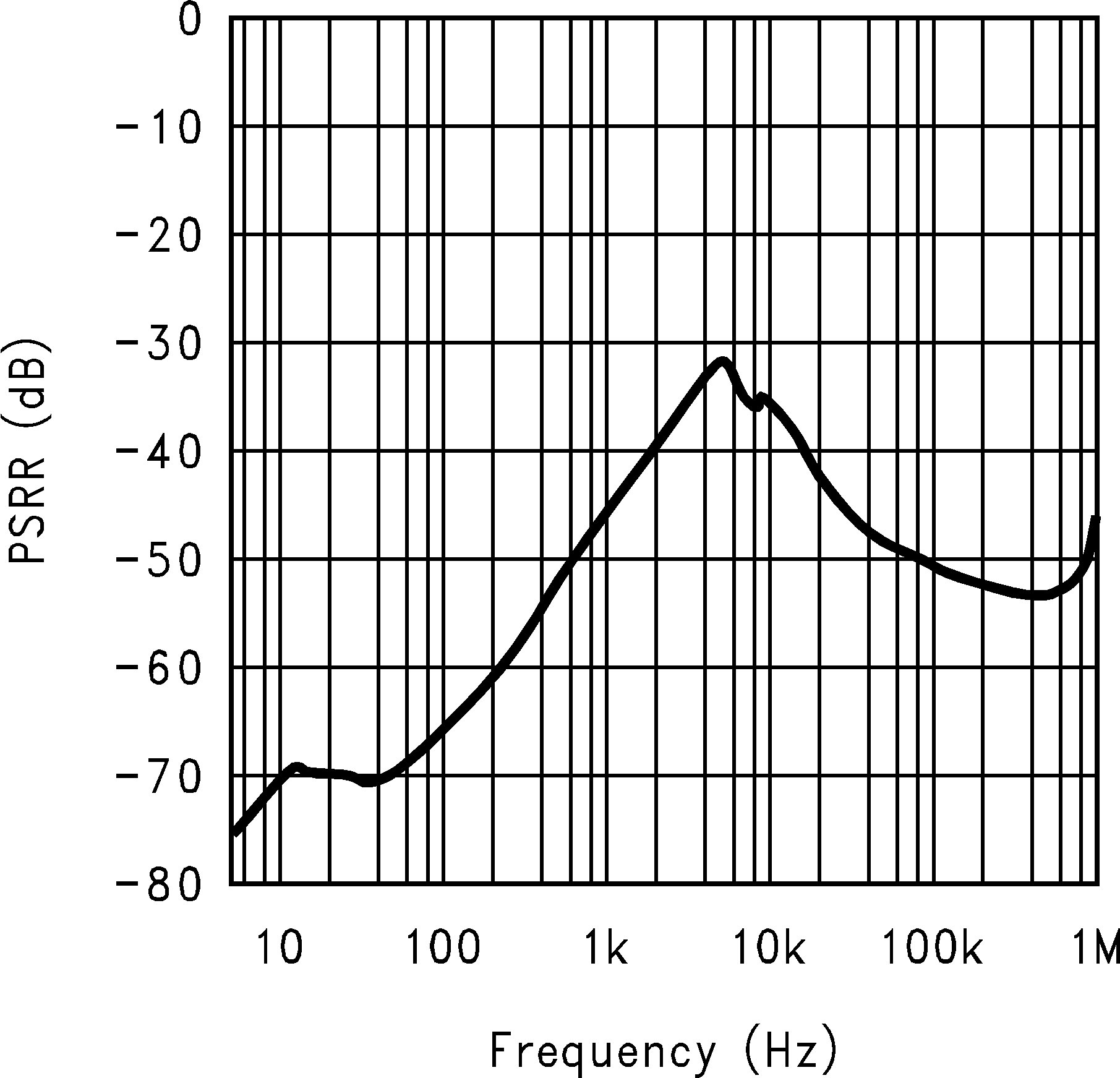 Figure 6. Power Supply Rejection Ratio
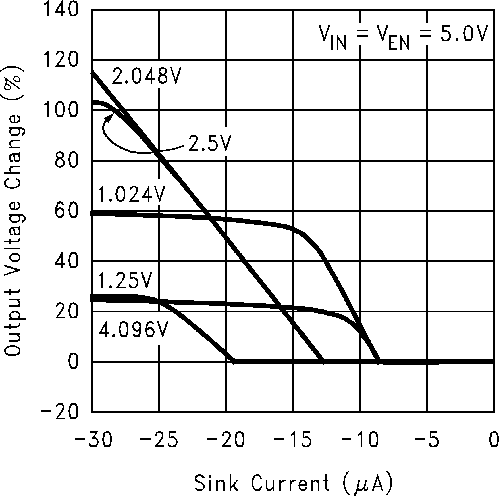 Figure 8. Output Voltage Change vs Sink Current (ISINK)
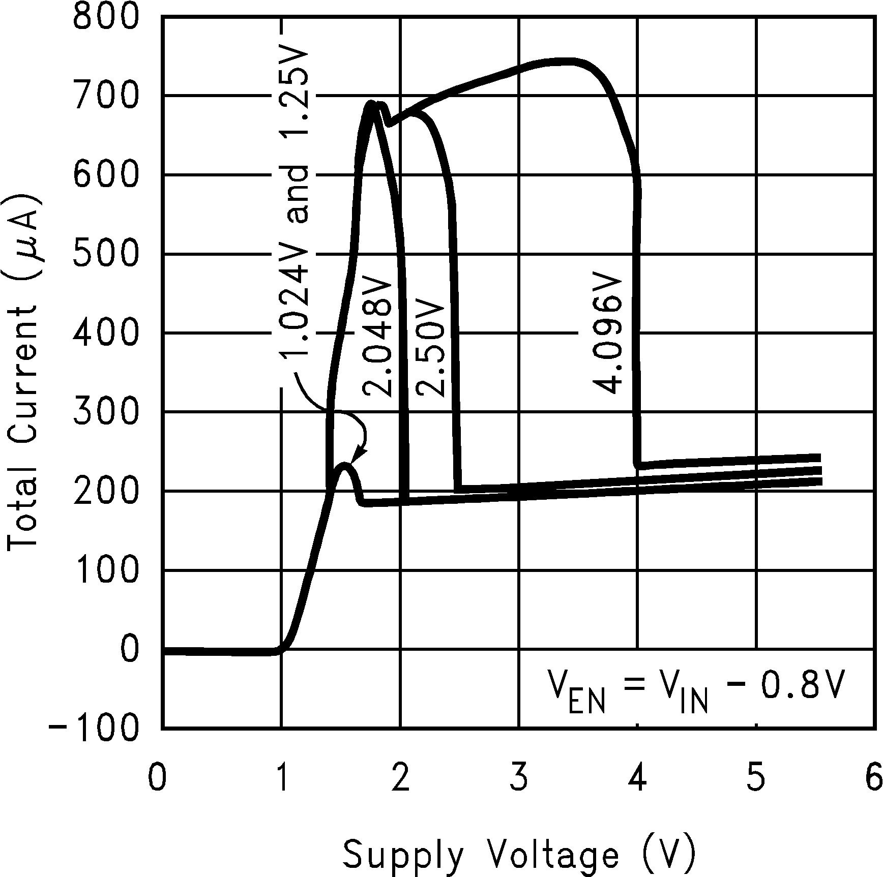 Figure 10. Total Current (IS(ON)) vs Supply Voltage
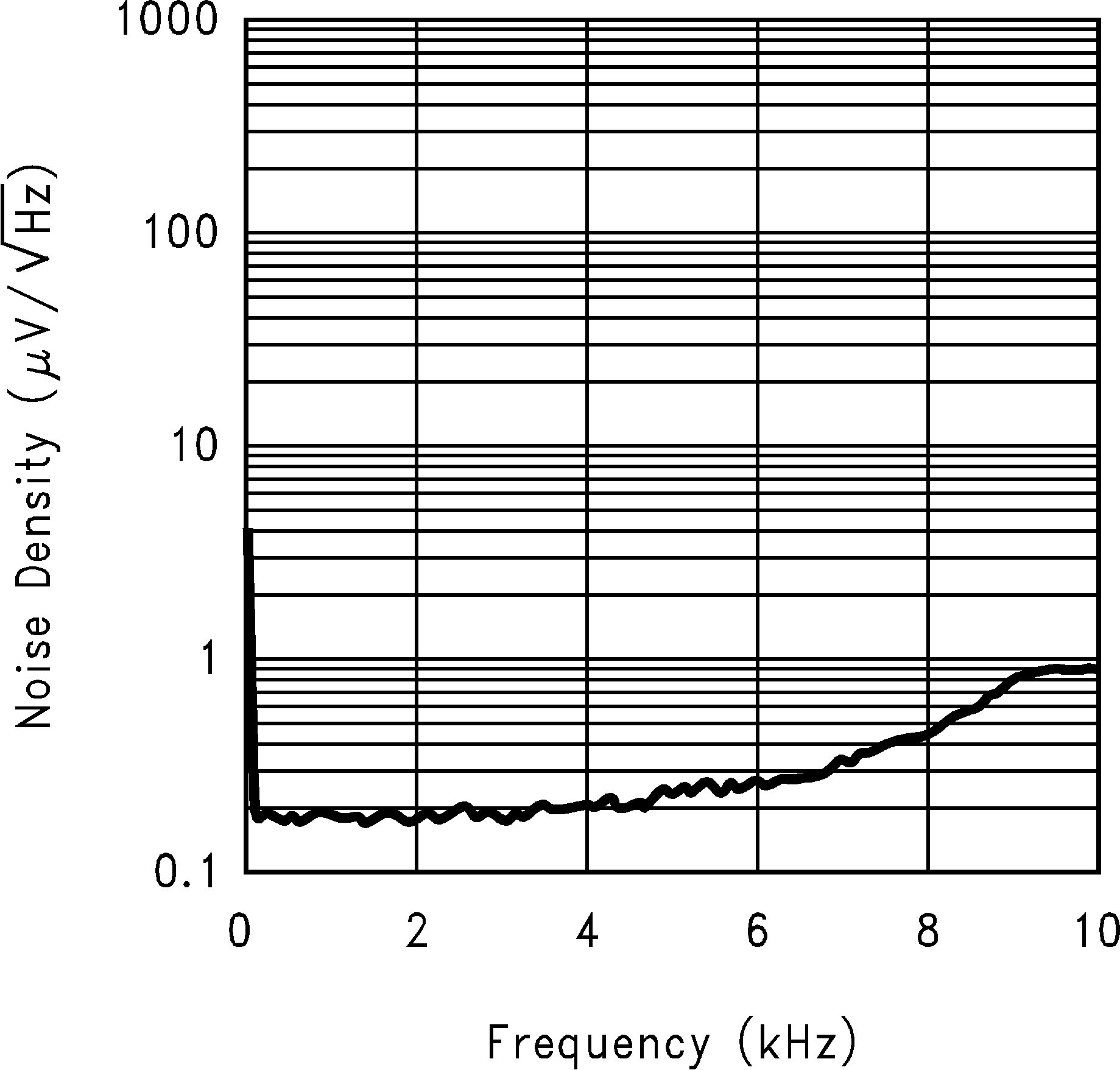 Figure 12. Spectral Noise Density (10 Hz to 100 kHz)
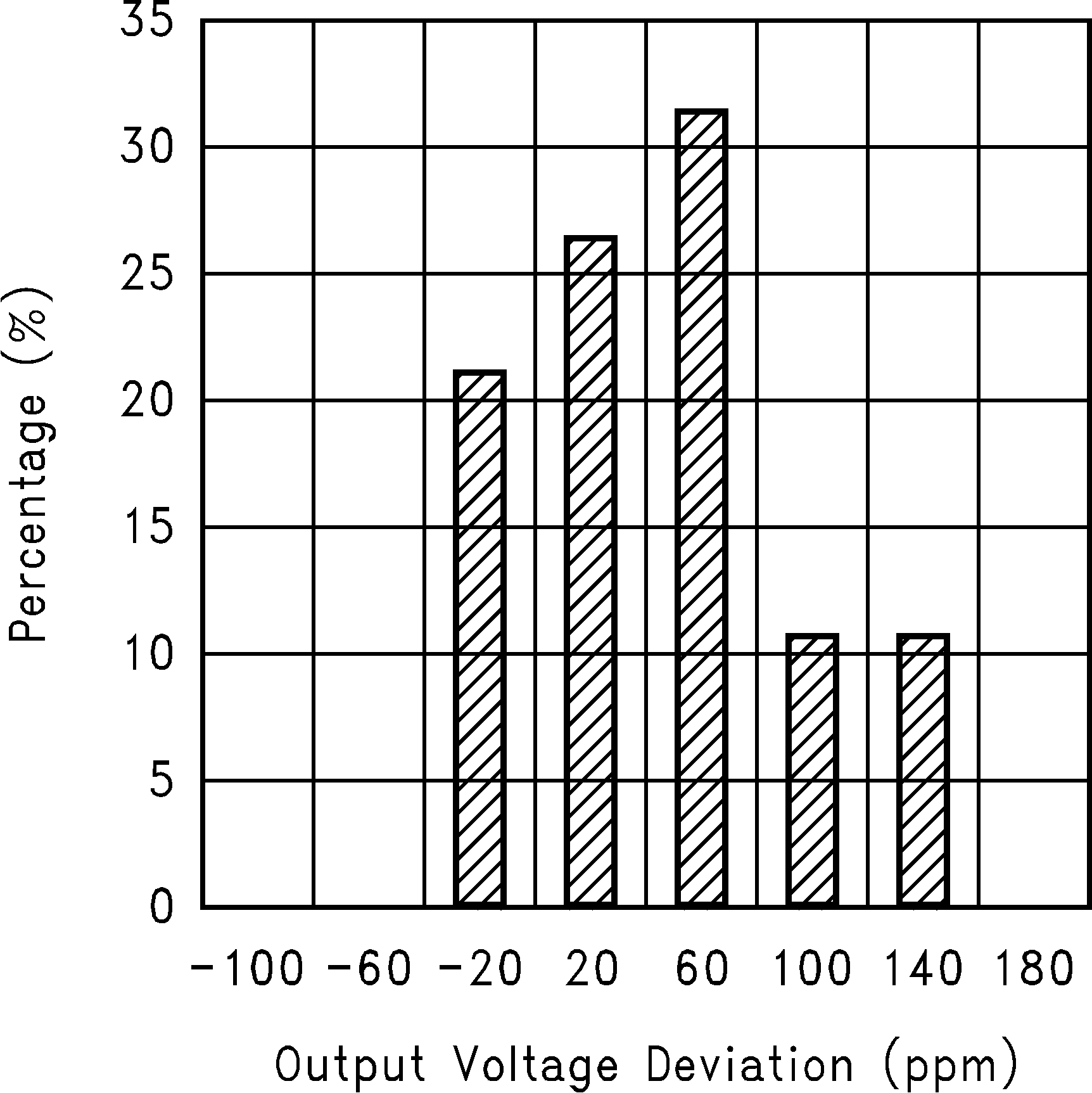 Figure 14. Long-Term Drift
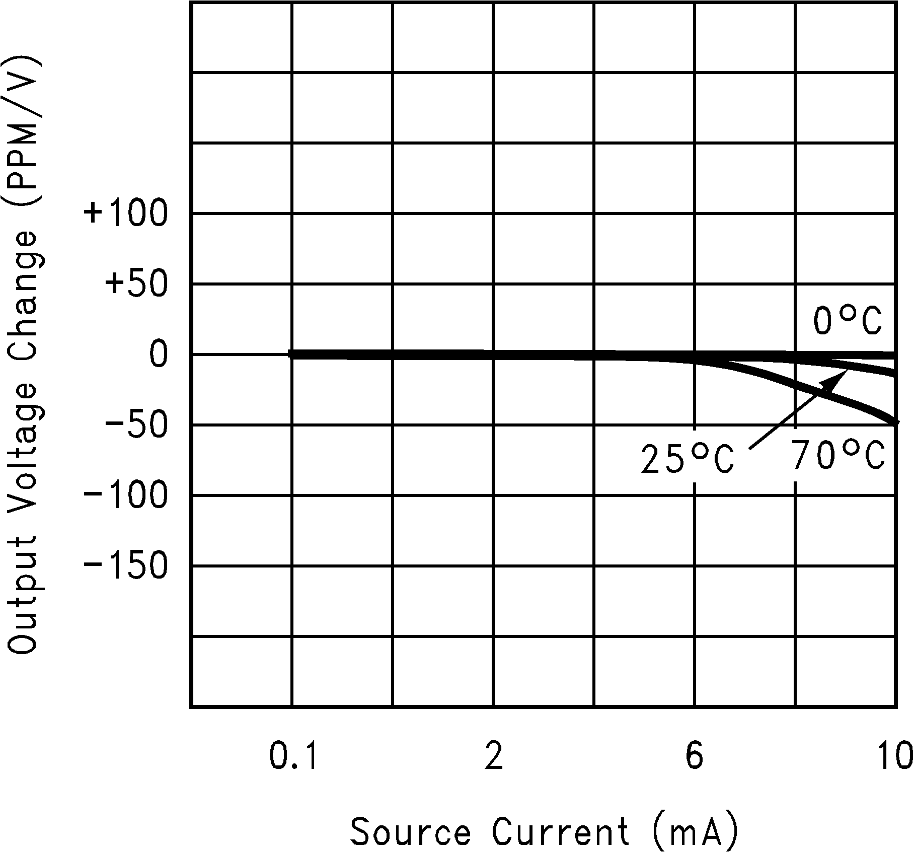 Figure 16. Output Voltage vs Load Current
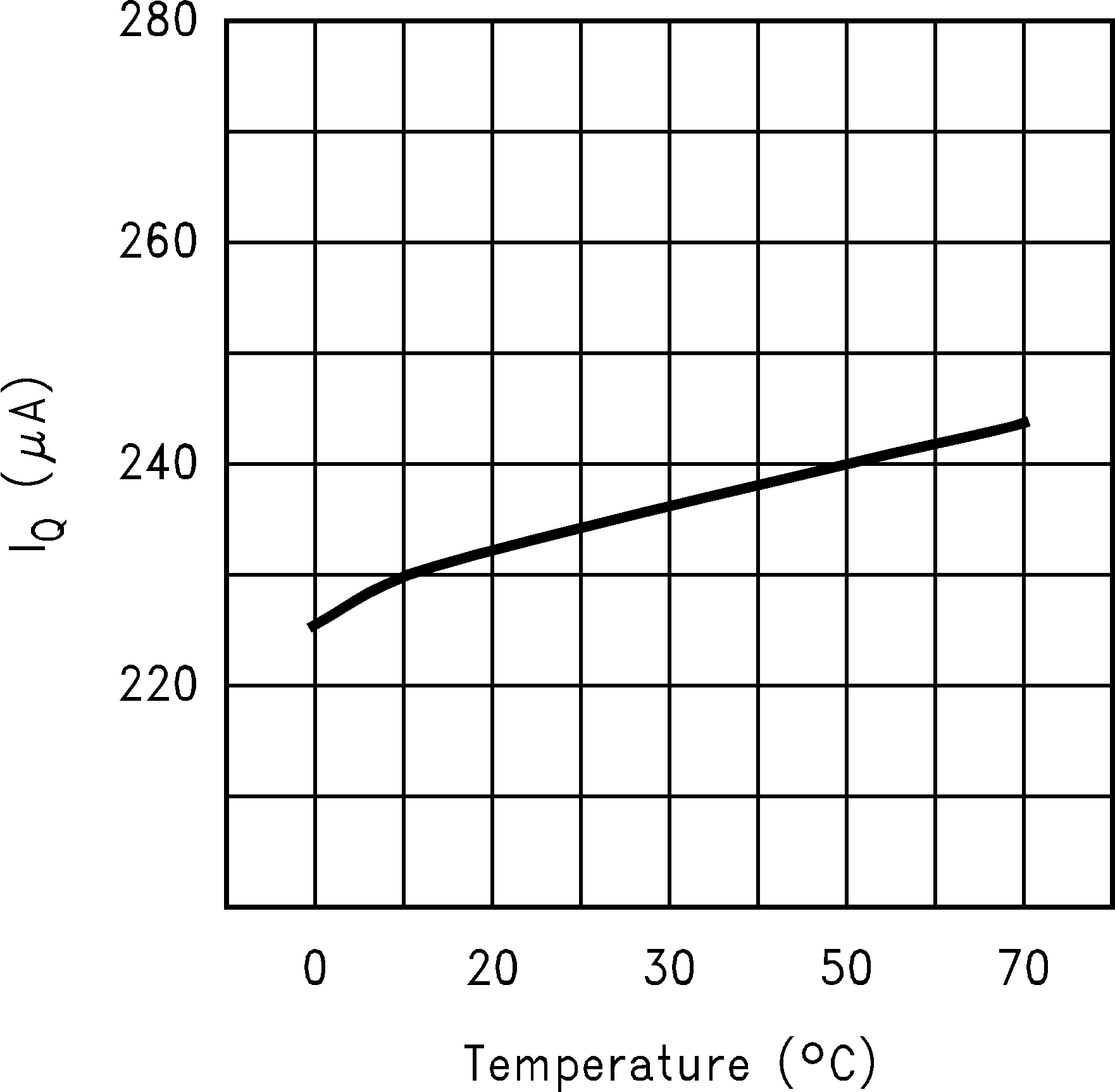 Figure 18. IQ vs Temperature
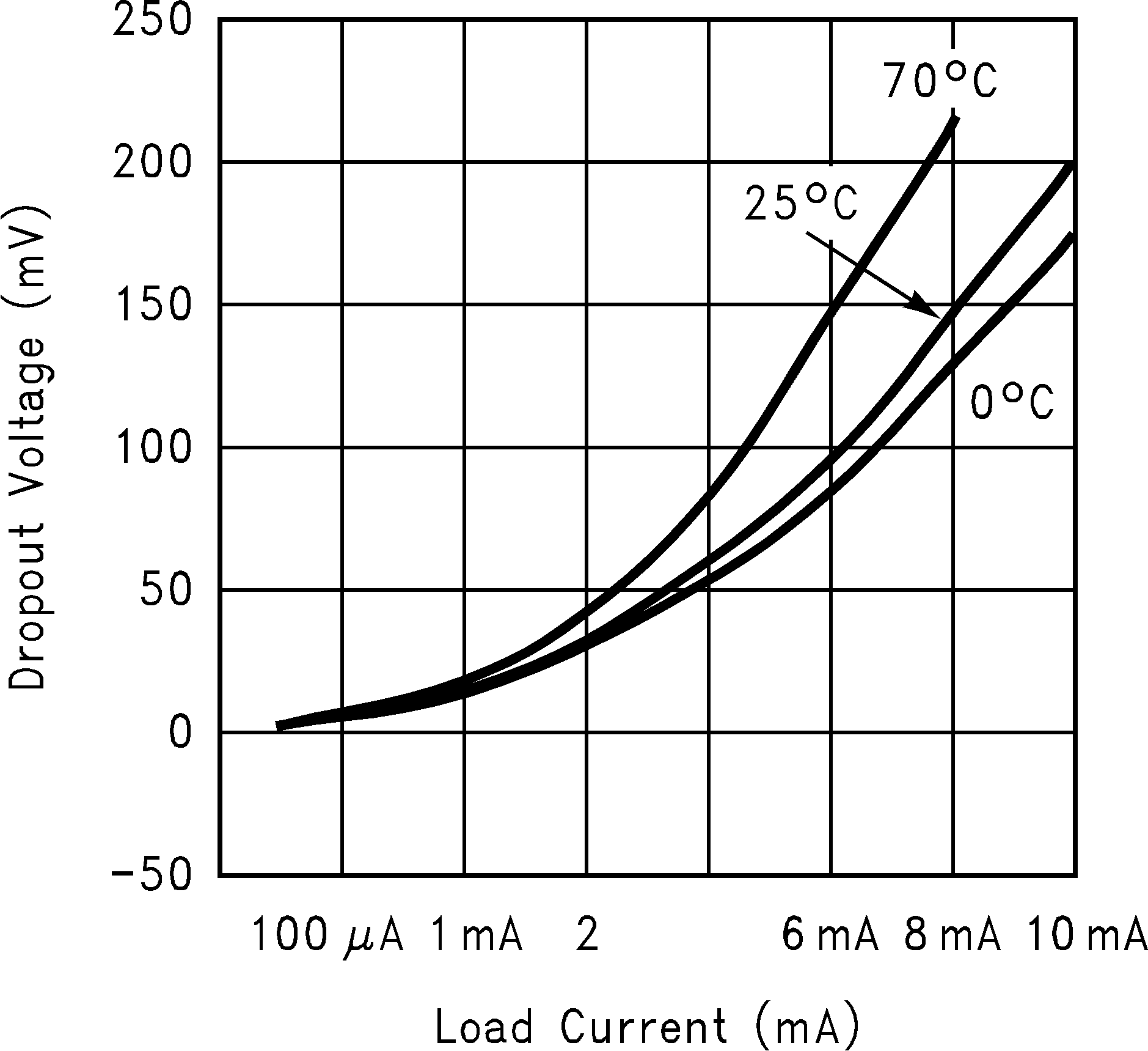 Figure 20. Dropout Voltage vs Load Current (VOUT) = 2 V