SNVS020H May 2000 – January 2016 LM431
PRODUCTION DATA.
- 1 Features
- 2 Applications
- 3 Description
- 4 Revision History
- 5 Pin Configuration and Functions
- 6 Specifications
- 7 Parameter Measurement Information
- 8 Detailed Description
- 9 Application and Implementation
- 10Power Supply Recommendations
- 11Layout
- 12Device and Documentation Support
- 13Mechanical, Packaging, and Orderable Information
Package Options
Mechanical Data (Package|Pins)
Thermal pad, mechanical data (Package|Pins)
Orderable Information
9 Application and Implementation
NOTE
Information in the following applications sections is not part of the TI component specification, and TI does not warrant its accuracy or completeness. TI’s customers are responsible for determining suitability of components for their purposes. Customers must validate and test their design implementation to confirm system functionality.
9.1 Application Information
The LM431 is an adjustable precision shunt voltage regulator with ensured temperature stability over the entire temperature range. For space critical applications, the LM431 is available in space saving SOIC-8, SOT-23 and TO-92 packages. The minimum operating current is 1 mA while the maximum operating current is 100 mA.
The typical thermal hysteresis specification is defined as the change in 25°C voltage measured after thermal cycling. The device is thermal cycled to temperature 0°C and then measured at 25°C. Next the device is thermal cycled to temperature 70°C and again measured at 25°C. The resulting VOUT delta shift between the 25°C measurements is thermal hysteresis. Thermal hysteresis is common in precision references and is induced by thermal-mechanical package stress. Changes in environmental storage temperature, operating temperature and board mounting temperature are all factors that can contribute to thermal hysteresis.
In a conventional shunt regulator application (Figure 12), an external series resistor (RS) is connected between the supply voltage and the LM431 cathode pin. RS determines the current that flows through the load (ILOAD) and the LM431 (IZ). Since load current and supply voltage may vary, RS must be small enough to supply at least the minimum acceptable IZ to the LM431 even when the supply voltage is at its minimum and the load current is at its maximum value. When the supply voltage is at its maximum and ILOAD is at its minimum, RS must be large enough so that the current flowing through the LM431 is less than 100 mA.
RS must be selected based on the supply voltage, (V+), the desired load and operating current, (ILOAD and IZ), and the output voltage, see Equation 1.

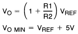
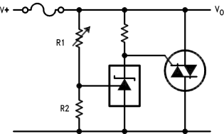
The LM431 output voltage can be adjusted to any value in the range of 2.5 V through 37 V. It is a function of the internal reference voltage (VREF) and the ratio of the external feedback resistors as shown in Figure 12. The output voltage is found using Equation 2.
where
- VO is the output voltage (also, cathode voltage, VZ). The actual value of the internal VREF is a function of VZ.
The corrected VREF is determined by Equation 3:
where
- VY = 2.5 V and ∆VZ = (VZ– VY)
- ΔVREF/ΔVZ is found in the Electrical Characteristics and is typically −1.4 mV/V for VZ raging from VREF to 10 V and –1 mV/V for VZ raging from 10 V to 36 V.
9.2 Typical Applications
9.2.1 Shunt Regulator
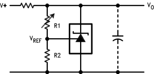

9.2.1.1 Design Requirements
Design a shunt regulator with the following requirements:
- V+ > VO
- VO = 5 V
Select RS (a resistor between V+ and VO) such that: 1 mA < IZ < 100 mA
9.2.1.2 Detailed Design Procedure
The resistor RS must be selected such that current IZ remains in the operational region of the part for the entire V+ range and load current range. The two extremes to consider are V+ at its minimum, and the load at its maximum, where RS must be small enough for IZ to remain above 1 mA. The other extreme is V+ at its maximum, and the load at its minimum, where RS must be large enough to maintain IZ < 100 mA. If unsure, try using 1 mA ≤ IR ≤ 10 mA as a starting point; just remember the value of IZ varies with input voltage and load.
Use Equation 4 and Equation 5 to set RS between RS_MIN and RS_MAX.


Set feedback resistors R1 and R2 for a resistor divider based on Equation 2 and reproduced in Equation 6
So, for a 5-V output voltage, VO, and VREF of 2.5 V, simple calculation yields R1/R2 = 1. Based on this, select
R1 = 1 kΩ and R2 = 1 kΩ.
9.2.1.3 Application Curves
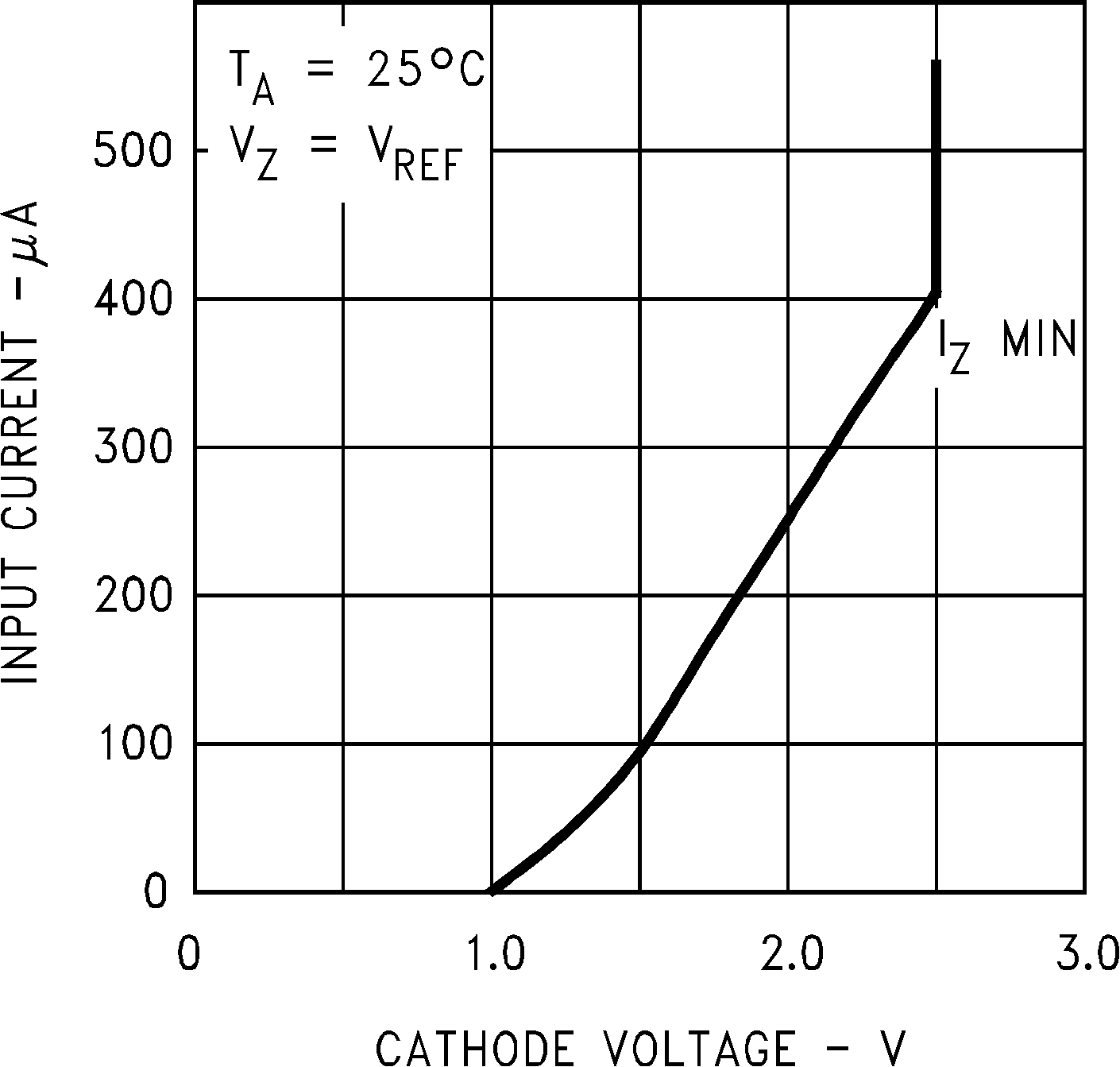
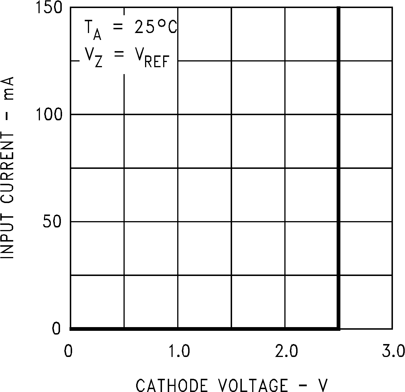 Figure 15. Input Current vs VZ
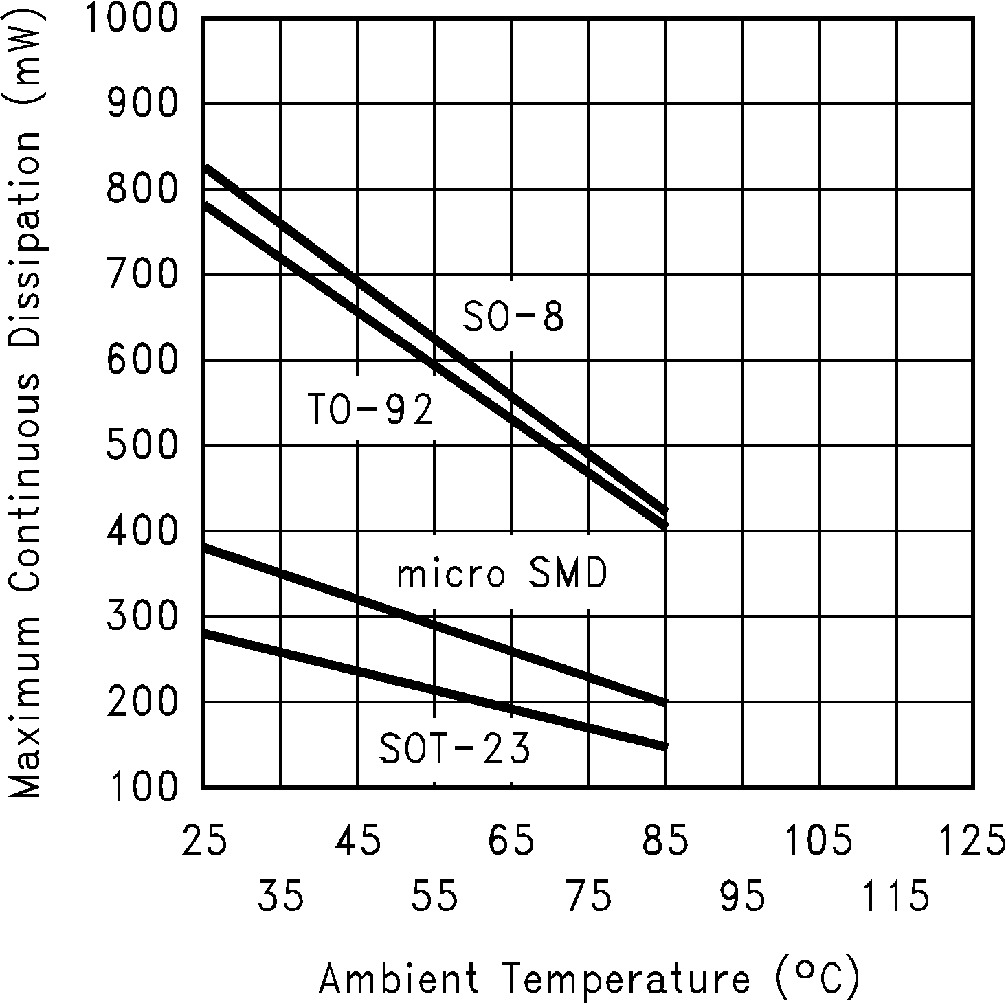 Figure 14. Thermal Information
9.2.2 Other Applications
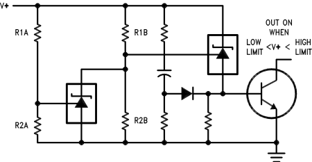
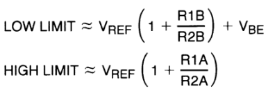
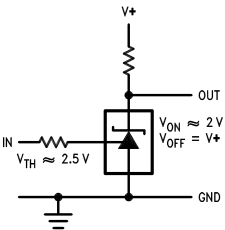 Figure 16. Single Supply Comparator With Temperature Compensated Threshold
