SNVS020H May 2000 – January 2016 LM431
PRODUCTION DATA.
- 1 Features
- 2 Applications
- 3 Description
- 4 Revision History
- 5 Pin Configuration and Functions
- 6 Specifications
- 7 Parameter Measurement Information
- 8 Detailed Description
- 9 Application and Implementation
- 10Power Supply Recommendations
- 11Layout
- 12Device and Documentation Support
- 13Mechanical, Packaging, and Orderable Information
Package Options
Mechanical Data (Package|Pins)
Thermal pad, mechanical data (Package|Pins)
Orderable Information
11 Layout
11.1 Layout Guidelines
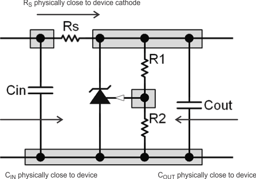
Place external components as close to the device as possible. Place RS close to the cathode, as well as the input bypass capacitor, if used. Keep feedback resistor close the device whenever possible.
11.2 Layout Example
 Figure 26. LM431 Layout Recommendation