SNAS470E October 2008 – November 2015 LM48100Q-Q1
PRODUCTION DATA.
- 1 Features
- 2 Applications
- 3 Description
- 4 Revision History
- 5 Pin Configuration and Functions
-
6 Specifications
- 6.1 Absolute Maximum Ratings
- 6.2 ESD Ratings
- 6.3 Recommended Operating Conditions
- 6.4 Thermal Information
- 6.5 Electrical Characteristics for VDD = 5 V
- 6.6 Electrical Characteristics for VDD = 5 V at Extended Temperature Limits
- 6.7 Electrical Characteristics for VDD = 3.6 V
- 6.8 Electrical Characteristics for VDD = 3.6 V at Extended Temperature Limits
- 6.9 I2C Interface Characteristics for VDD = 5 V, 2.2 V ≤ I2C VDD ≤ 5.5 V
- 6.10 I2C Interface Characteristics for VDD = 5 V, 1.8 V ≤ I2C VDD ≤ 2.2 V
- 6.11 Typical Characteristics
-
7 Detailed Description
- 7.1 Overview
- 7.2 Functional Block Diagram
- 7.3 Feature Description
- 7.4 Device Functional Modes
- 7.5 Programming
- 7.6 Register Maps
- 8 Application and Implementation
- 9 Power Supply Recommendations
- 10Layout
- 11Device and Documentation Support
- 12Mechanical, Packaging, and Orderable Information
Package Options
Mechanical Data (Package|Pins)
- PWP|14
Thermal pad, mechanical data (Package|Pins)
- PWP|14
Orderable Information
8 Application and Implementation
NOTE
Information in the following applications sections is not part of the TI component specification, and TI does not warrant its accuracy or completeness. TI’s customers are responsible for determining suitability of components for their purposes. Customers should validate and test their design implementation to confirm system functionality.
8.1 Application Information
The LM48100Q-Q1 is a single-supply, mono, bridge-tied load amplifier with I2C volume control, ideal for automotive applications. It integrates a comprehensive output fault detection system, which can sense the load conditions, protecting the device during short circuit events and detecting open circuit conditions. High power supply rejection ratio allows the device to operate in noisy environments without additional power supply conditioning. The LM48100Q-Q1 features dual audio inputs that can mixed or multiplexed to the device output. Each input path has its own independent, 32-step volume control. The mixer, volume control and device mode select are controlled through an I2C compatible interface. The LM48100Q-Q1 device has an I2C selectable low power shutdown mode that disables the device, reducing quiescent current consumption to 0.01μA
8.2 Typical Application
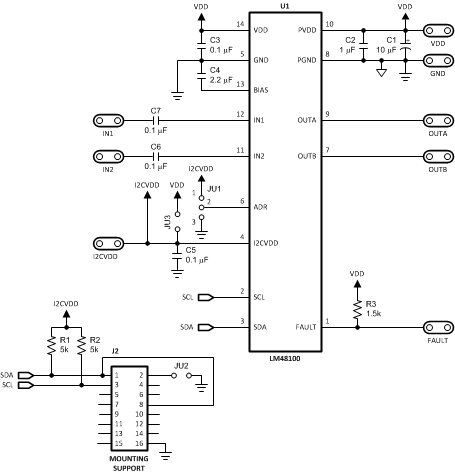
 Figure 15. LM48100Q-Q1 Demo Board Schematic
8.2.1 Design Requirements
For this design example, use the parameters listed in Table 8 as the input parameters.
Table 8. Design Parameters
| DESIGN PARAMETER | EXAMPLE VALUES |
|---|---|
| Supply Voltage Range | 3 V to 5.5 V |
| I2C Supply Voltage Range | 1.8 V to 5.5 V |
| Temperature Range | –40 °C to 105 °C |
| Input Voltage Range | –0.3 V to VDD = 0.3 V |
8.2.2 Detailed Design Procedure
8.2.2.1 Power Supply Bypassing/Filtering
Proper power supply bypassing is critical for low noise performance and high PSRR. Place the supply bypass capacitors as close to the device as possible. Place a 1-µF ceramic capacitor from VDD to GND. Additional bulk capacitance may be added as required.
8.2.2.2 Input Capacitor Selection
Input capacitors may be required for some applications, or when the audio source is single-ended. Input capacitors block the DC component of the audio signal, eliminating any conflict between the DC component of the audio source and the bias voltage of the LM48100Q-Q1. The input capacitors create a high-pass filter with the input resistors RIN. The –3 dB point of the high-pass filter is found using Equation 4.
where
- RIN is given in the Electrical Characteristics tables found in Specifications
High pass filtering the audio signal helps protect the speakers. When the LM48100Q-Q1 is using a single-ended source, power supply noise on the ground is seen as an input signal. Setting the high-pass filter point above the power supply noise frequencies, filters out the noise such that it is not amplified and heard on the output. Capacitors with a tolerance of 10% or better are recommended for impedance matching and improved PSRR.
8.2.2.3 Bias Capacitor Selection
The LM48100Q-Q1 internally generates a VDD/2 common-mode bias voltage. The BIAS capacitor CBIAS, improves PSRR and THD+N by reducing noise at the BIAS node. Use a 2.2-µF ceramic placed as close to the device as possible.
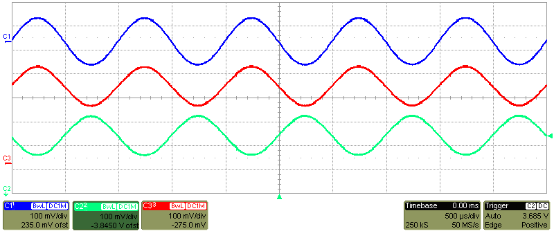
8.2.3 Application Curve
