SNVS484H January 2007 – July 2015 LM5001 , LM5001-Q1
PRODUCTION DATA.
- 1 Features
- 2 Applications
- 3 Description
- 4 Revision History
- 5 Pin Configuration and Functions
- 6 Specifications
- 7 Detailed Description
- 8 Applications and Implementation
- 9 Layout
- 10Device and Documentation Support
- 11Mechanical, Packaging, and Orderable Information
Package Options
Mechanical Data (Package|Pins)
Thermal pad, mechanical data (Package|Pins)
Orderable Information
7 Detailed Description
7.1 Overview
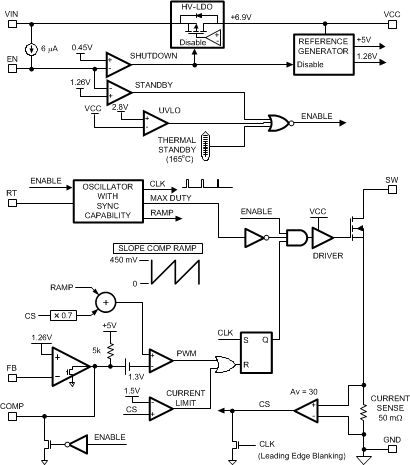
The LM5001 high voltage switching regulator features all the functions necessary to implement an efficient boost, flyback, SEPIC or forward current mode power converter. The operation can be best understood by referring to the block diagram. At the start of each cycle, the oscillator sets the driver logic and turns on the power MOSFET to conduct current through the inductor or transformer. The peak current in the MOSFET is controlled by the voltage at the COMP pin. The COMP voltage increases with larger loads and decrease with smaller loads. This voltage is compared with the sum of a voltage proportional to the power MOSFET current and an internally generated Slope Compensation ramp. Slope Compensation is used in current mode PWM architectures to eliminate sub-harmonic current oscillation that occurs with static duty cycles greater than 50%. When the summed signal exceeds the COMP voltage, the PWM comparator resets the driver logic, turning off the power MOSFET. The driver logic is then set by the oscillator at the end of the switching cycle to initiate the next power period.
The LM5001 has dedicated protection circuitry to protect the IC from abnormal operating conditions. Cycle-by-cycle current limiting prevents the power MOSFET current from exceeding 1 A. This feature can also be used to soft-start the regulator. Thermal Shutdown circuitry holds the driver logic in reset when the die temperature reaches 165°C, and returns to normal operation when the die temperature drops by approximately 20°C. The EN pin can be used as an input voltage undervoltage lockout (UVLO) during start-up to prevent operation with less than the minimum desired input voltage.
7.2 Functional Block Diagram

7.3 Feature Description
7.3.1 High-Voltage VCC Regulator
The LM5001 VCC Low Drop Out (LDO) regulator allows the LM5001 to operate at the lowest possible input voltage. The VCC pin voltage is very nearly equal to the input voltage from 2.8 V up to approximately 6.9 V. As the input voltage continues to increase, the VCC pin voltage is regulated at the 6.9 V set-point. The total input operating range of the VCC LDO regulator is 3.1 V to 75 V.
The output of the VCC regulator is current limited to 20 mA. During power up, the VCC regulator supplies current into the required decoupling capacitor (0.47 µF or greater ceramic capacitor) at the VCC pin. When the voltage at the VCC pin exceeds the VCC UVLO threshold of 2.8 V and the EN pin is greater than 1.26 V the PWM controller is enabled and switching begins. The controller remains enabled until VCC falls below 2.7 V or the EN pin falls below 1.16 V.
An auxiliary supply voltage can be applied to the VCC pin to reduce the IC power dissipation. If the auxiliary voltage is greater than 6.9 V, the internal regulator essentially shuts off, and internal power dissipation decreases by the VIN voltage times the operating current. The overall converter efficiency improves if the VIN voltage is much higher than the auxiliary voltage. The externally applied VCC voltage should not exceed 14 V. The VCC regulator series pass MOSFET includes a body diode (Functional Block Diagram) between VCC and VIN that should not be forward biased in normal operation. Therefore, the auxiliary VCC voltage should never exceed the VIN voltage.
In high voltage applications extra care should be taken to ensure the VIN pin does not exceed the absolute maximum voltage rating of 76 V. Voltage ringing on the VIN line during line transients that exceeds the Absolute Maximum Ratings damages the IC. Both careful PC board layout and the use of quality bypass capacitors located close to the VIN and GND pins are essential.
7.3.2 Oscillator
A single external resistor connected between RT and GND pins sets the LM5001 oscillator frequency. To set a desired oscillator frequency (FSW), the necessary value for the RT resistor can be calculated from:

The tolerance of the external resistor and the frequency tolerance indicated in the Electrical Characteristics must be taken into account when determining the worst case frequency range.
7.3.3 External Synchronization
The LM5001 can be synchronized to the rising edge of an external clock. The external clock must have a higher frequency than the free running oscillator frequency set by the RT resistor. The clock signal should be coupled through a 100 pF capacitor into the RT pin. A peak voltage level greater than 2.6 V at the RT pin is required for detection of the sync pulse. The DC voltage across the RT resistor is internally regulated at 1.5 V. The negative portion of the AC voltage of the synchronizing clock is clamped to this 1.5 V by an amplifier inside the LM5001 with ~100 Ω output impedance. Therefore, the AC pulse superimposed on the RT resistor must have positive pulse amplitude of 1.1 V or greater to successfully synchronize the oscillator. The sync pulse width measured at the RT pin should have a duration greater than 15 ns and less than 5% of the switching period. The sync pulse rising edge initiates the internal CLK signal rising edge, which turns off the power MOSFET. The RT resistor is always required, whether the oscillator is free running or externally synchronized. The RT resistor should be located very close to the device and connected directly to the RT and GND pins of the LM5001.
7.3.4 Enable / Standby
The LM5001 contains a dual level Enable circuit. When the EN pin voltage is below 450 mV, the IC is in a low current shutdown mode with the VCC LDO disabled. When the EN pin voltage is raised above the shutdown threshold but below the 1.26 V standby threshold, the VCC LDO regulator is enabled, while the remainder of the IC is disabled. When the EN pin voltage is raised above the 1.26 V standby threshold, all functions are enabled and normal operation begins. An internal 6 µA current source pulls up the EN pin to activate the IC when the EN pin is left disconnected.
An external set-point resistor divider from VIN to GND can be used to determine the minimum operating input range of the regulator. The divider must be designed such that the EN pin exceeds the 1.26 V standby threshold when VIN is in the desired operating range. The internal 6 µA current source should be included when determining the resistor values. The shutdown and standby thresholds have 100 mV hysteresis to prevent noise from toggling between modes. When the VIN voltage is below 3.5 VDC during start-up and the operating temperature is below –20°C, the EN pin should have a pull-up resistor provides 2 µA or greater current. The EN pin is internally protected by a 6 V Zener diode through a 1 kΩ resistor. The enabling voltage may exceed the Zener voltage, however the Zener current should be limited to less than 4 mA.
7.3.5 Error Amplifier and PWM Comparator
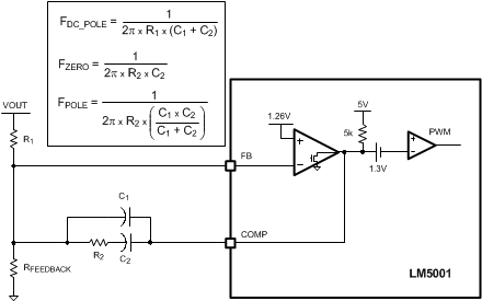
An internal high gain error amplifier generates an error signal proportional to the difference between the regulated output voltage and an internal precision reference. The output of the error amplifier is connected to the COMP pin allowing the user to add loop compensation, typically a Type II network, as illustrated in Figure 13. This network creates a low frequency pole that rolls off the high DC gain of the amplifier, which is necessary to accurately regulate the output voltage. FDC_POLE is the closed loop unity gain (0 dB) frequency of this pole. A zero provides phase boost near the closed loop unity gain frequency, and a high frequency pole attenuates switching noise. The PWM comparator compares the current sense signal from the current sense amplifier to the error amplifier output voltage at the COMP pin.
 Figure 13. Type II Compensator
When isolation between primary and secondary circuits is required, the Error Amplifier is usually disabled by connecting the FB pin to GND. This allows the COMP pin to be driven directly by the collector of an opto-coupler. In isolated designs the external error amplifier is located on the secondary circuit and drives the opto-coupler LED. The compensation network is connected to the secondary side error amplifier. An example of an isolated regulator with an opto-coupler is shown in Figure 19.
7.3.6 Current Amplifier and Slope Compensation
The LM5001 employs peak current mode control which also provides a cycle-by-cycle over current protection feature. An internal 50 mΩ current sense resistor measures the current in the power MOSFET source. The sense resistor voltage is amplified 30 times to provide a 1.5 V/A signal into the current limit comparator. Current limiting is initiated if the internal current limit comparator input exceeds the 1.5 V threshold, corresponding to 1 A. When the current limit comparator is triggered, the SW output pin immediately switches to a high impedance state.
The current sense signal is reduced to a scale factor of 1.05 V/A for the PWM comparator signal. The signal is then summed with a 450 mV peak slope compensation ramp. The combined signal provides the PWM comparator with a control signal that reaches 1.5 V when the MOSFET current is 1 A. For duty cycles greater than 50%, current mode control circuits are subject to sub-harmonic oscillation (alternating between short and long PWM pulses every other cycle). Adding a fixed slope voltage ramp signal (slope compensation) to the current sense signal prevents this oscillation. The 450 mV ramp (zero volts when the power MOSFET turns on, and 450 mV at the end of the PWM clock cycle) adds a fixed slope to the current sense ramp to prevent oscillation.
To prevent erratic operation at low duty cycle, a leading edge blanking circuit attenuates the current sense signal when the power MOSFET is turned on. When the MOSFET is initially turned on, current spikes from the power MOSFET drain-source and gate-source capacitances flow through the current sense resistor. These transient currents normally cease within 50 ns with proper selection of rectifier diodes and proper PC board layout.
7.3.7 Thermal Protection
Internal Thermal Shutdown circuitry is provided to protect the IC in the event the maximum junction temperature is exceeded. When the 165°C junction temperature threshold is reached, the regulator is forced into a low power standby state, disabling all functions except the VCC regulator. Thermal hysteresis allows the IC to cool down before it is re-enabled. Note that since the VCC regulator remains functional during this period, the soft-start circuit shown in Figure 17 should be augmented if soft-start from Thermal Shutdown state is required.
7.3.8 Power MOSFET
The LM5001 switching regulator includes an N-Channel MOSFET with 440-mΩ on-resistance. The on-resistance of the LM5001 MOSFET varies with temperature as shown in the Typical Characteristics graph. The typical total gate charge for the MOSFET is 4.5 nC which is supplied from the VCC pin when the MOSFET is turned on.