SNVS484H January   2007  – July 2015 LM5001 , LM5001-Q1

PRODUCTION DATA.  

  1. Features
  2. Applications
  3. Description
  4. Revision History
  5. Pin Configuration and Functions
  6. Specifications
    1. 6.1 Absolute Maximum Ratings
    2. 6.2 ESD Ratings
    3. 6.3 Recommended Operating Conditions
    4. 6.4 Thermal Information
    5. 6.5 Electrical Characteristics
    6. 6.6 Typical Characteristics
  7. Detailed Description
    1. 7.1 Overview
    2. 7.2 Functional Block Diagram
    3. 7.3 Feature Description
      1. 7.3.1 High-Voltage VCC Regulator
      2. 7.3.2 Oscillator
      3. 7.3.3 External Synchronization
      4. 7.3.4 Enable / Standby
      5. 7.3.5 Error Amplifier and PWM Comparator
      6. 7.3.6 Current Amplifier and Slope Compensation
      7. 7.3.7 Thermal Protection
      8. 7.3.8 Power MOSFET
  8. Applications and Implementation
    1. 8.1 Application Information
      1. 8.1.1 VIN
      2. 8.1.2 SW Pin
      3. 8.1.3 EN / UVLO Voltage Divider Selection
      4. 8.1.4 Soft-Start
    2. 8.2 Typical Applications
      1. 8.2.1 Non-Isolated Flyback
      2. 8.2.2 Isolated Flyback
      3. 8.2.3 Boost
      4. 8.2.4 24-V SEPIC
      5. 8.2.5 12-V Automotive SEPIC
  9. Layout
    1. 9.1 Layout Guidelines
  10. 10Device and Documentation Support
    1. 10.1 Related Links
    2. 10.2 Trademarks
    3. 10.3 Electrostatic Discharge Caution
    4. 10.4 Glossary
  11. 11Mechanical, Packaging, and Orderable Information

Package Options

Mechanical Data (Package|Pins)
Thermal pad, mechanical data (Package|Pins)
Orderable Information

6 Specifications

6.1 Absolute Maximum Ratings

over operating free-air temperature range (unless otherwise noted)
MIN MAX UNIT
VIN to GND 76 V
SW to GND (Steady State) –0.3 76 V
VCC, EN to GND 14 V
COMP, FB, RT to GND –0.3 7 V
Maximum Junction Temperature 150 °C
Storage Temperature Range, Tstg -65 150 °C

6.2 ESD Ratings

VALUE UNIT
V(ESD) Electrostatic discharge Human-body model (HBM), per AEC Q100-002(1) ±2000 V
Charged-device model (CDM), per AEC Q100-011 ±750
(1) AEC Q100-002 indicates that HBM stressing shall be in accordance with the ANSI/ESDA/JEDEC JS-001 specification.

6.3 Recommended Operating Conditions

MIN NOM MAX UNIT
VIN 3.1 75 V
Operating Junction Temperature −40 125 °C

6.4 Thermal Information

THERMAL METRIC LM5001-Q1 LM5001 UNIT
SOIC SOIC WSON
(8 PINS)
RθJA Junction-to-ambient thermal resistance 140 140 40 °C/W
RθJCtop Junction-to-case (top) thermal resistance 32 32 4.5

6.5 Electrical Characteristics

Minimum and Maximum limits are ensured through test, design, or statistical correlation, over the junction temperature (TJ) range of –40°C to +125°C. Typical values represent the most likely parametric norm at TJ = 25°C, and are provided for reference purposes only. VVIN = 10 V, RRT = 48.7 kΩ unless otherwise stated(1).
SYMBOL PARAMETER TEST CONDITIONS MIN TYP MAX UNIT
Startup Regulator
VVCC-REG VCC Regulator Output 6.55 6.85 7.15 V
VCC Current Limit VVCC = 6 V 15 20 mA
VCC UVLO Threshold VVCC increasing 2.6 2.8 3 V
VCC Undervoltage Hysteresis 0.1
Bias Current (IIN) VFB = 1.5 V 3.1 4.5 mA
IQ Shutdown Current (IIN) VEN = 0V 95 130 µA
EN Thresholds
EN Shutdown Threshold VEN increasing 0.25 0.45 0.65 V
EN Shutdown Hysteresis 0.1
EN Standby Threshold VEN increasing 1.2 1.26 1.32
EN Standby Hysteresis 0.1
EN Current Source 6 µA
MOSFET Characteristics
MOSFET RDS(ON) plus
Current Sense Resistance
LM5001 ID = 0.5 A 490 800
LM5001-Q1 490 880
MOSFET Leakage Current VSW = 75 V 0.05 5 µA
MOSFET Gate Charge VVCC = 6.9 V 4.5 nC
Current Limit
ILIM Cycle by Cycle Current Limit 0.8 1.0 1.2 A
Cycle by Cycle Current Limit Delay 100 200 ns
Oscillator
FSW1 Frequency1 RRT = 48.7 kΩ 225 260 295 KHz
FSW2 Frequency2 RRT = 15.8 kΩ 660 780 900
VRT-SYNC SYNC Threshold 2.2 2.6 3.2 V
SYNC Pulse Width Minimum VRT > VRT-SYNC + 0.5 V 15 ns
PWM Comparator
Maximum Duty Cycle 80% 85% 90%
Min On-time VCOMP > VCOMP-OS 35 ns
Min On-time VCOMP < VCOMP-OS 0
VCOMP-OS COMP to PWM Comparator Offset 0.9 1.30 1.55 V
Error Amplifier
VFB-REF Feedback Reference Voltage Internal reference
VFB = VCOMP
1.241 1.260 1.279 V
FB Bias Current 10 nA
DC Gain 72 dB
COMP Sink Current VCOMP = 250 mV 2.5 mA
COMP Short Circuit Current VFB = 0, VCOMP = 0 0.9 1.2 1.5
COMP Open Circuit Voltage VFB = 0 4.8 5.5 6.2 V
COMP to SW Delay 50 ns
Unity Gain Bandwidth 3 MHz
Thermal Shutdown
TSD Thermal Shutdown Threshold 165 °C
Thermal Shutdown Hysteresis 20
(1) Min and Max limits are 100% production tested at 25°C. Limits over the operating temperature range are specified through correlation using Statistical Quality Control (SQC) methods. Limits are used to calculate TI’s Average Outgoing Quality Level (AOQL).

6.6 Typical Characteristics
LM5001 LM5001-Q1 20215718.png
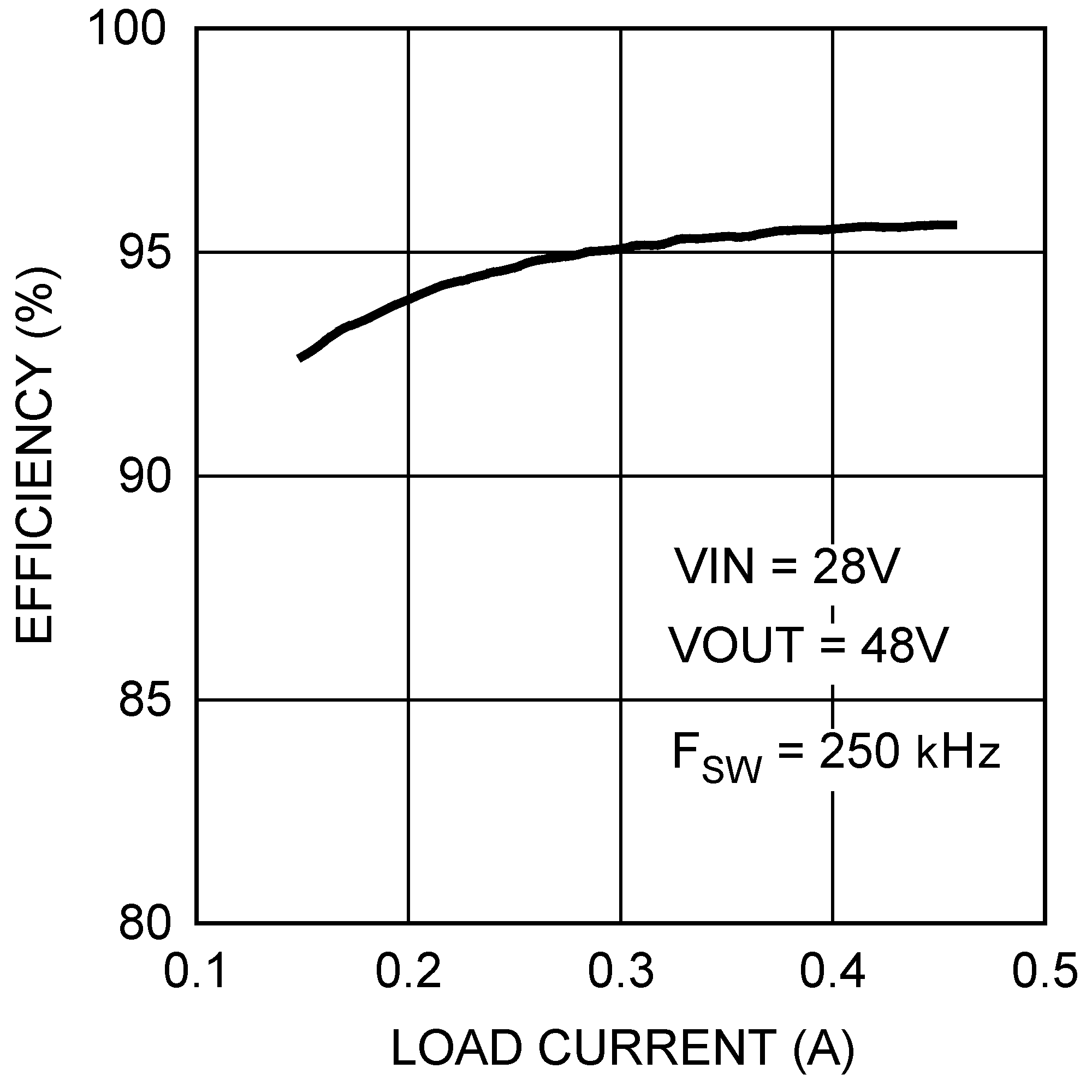
Figure 1. Efficiency, Boost Converter
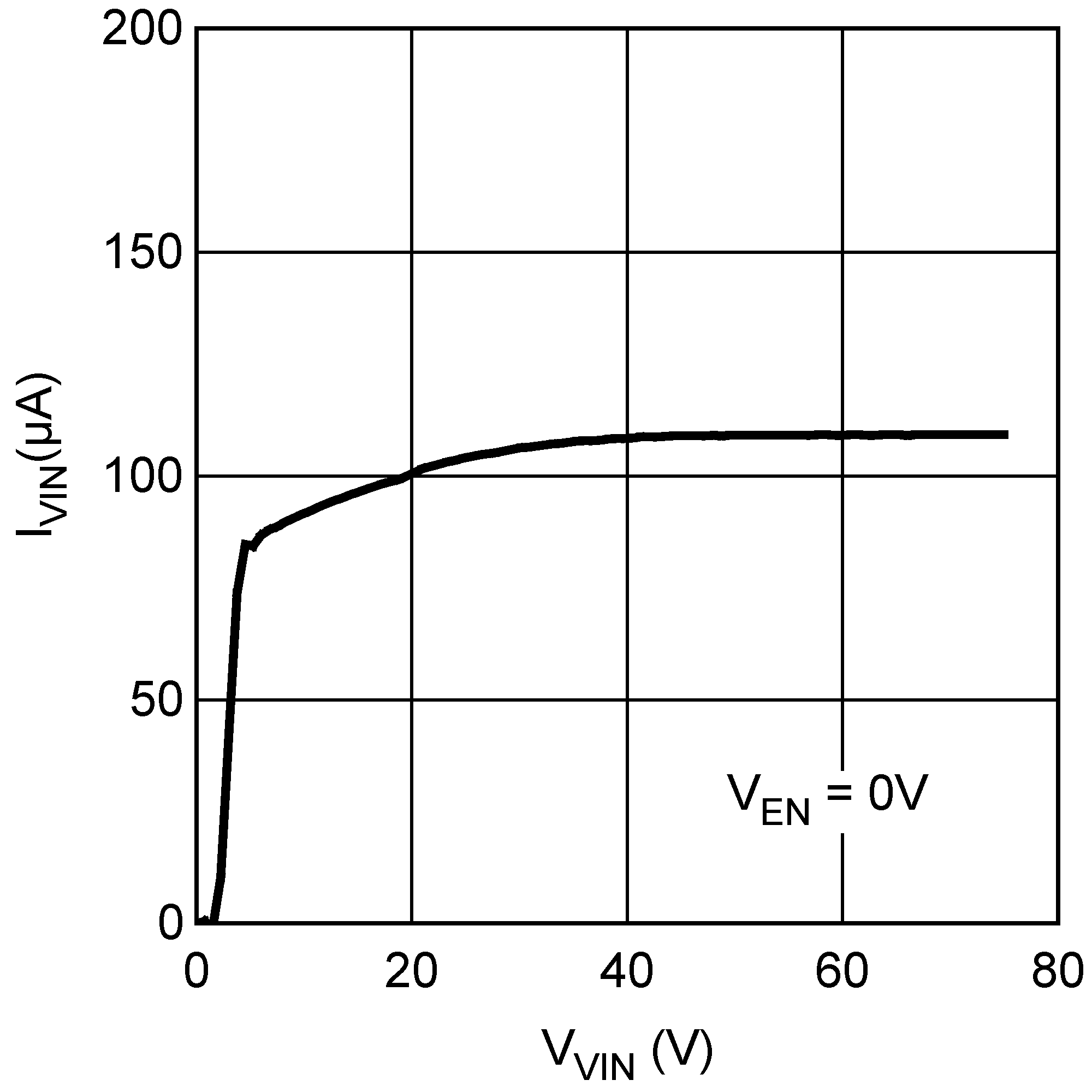
LM5001 LM5001-Q1 20215720.png
Figure 3. IQ (Non-Switching) vs VIN
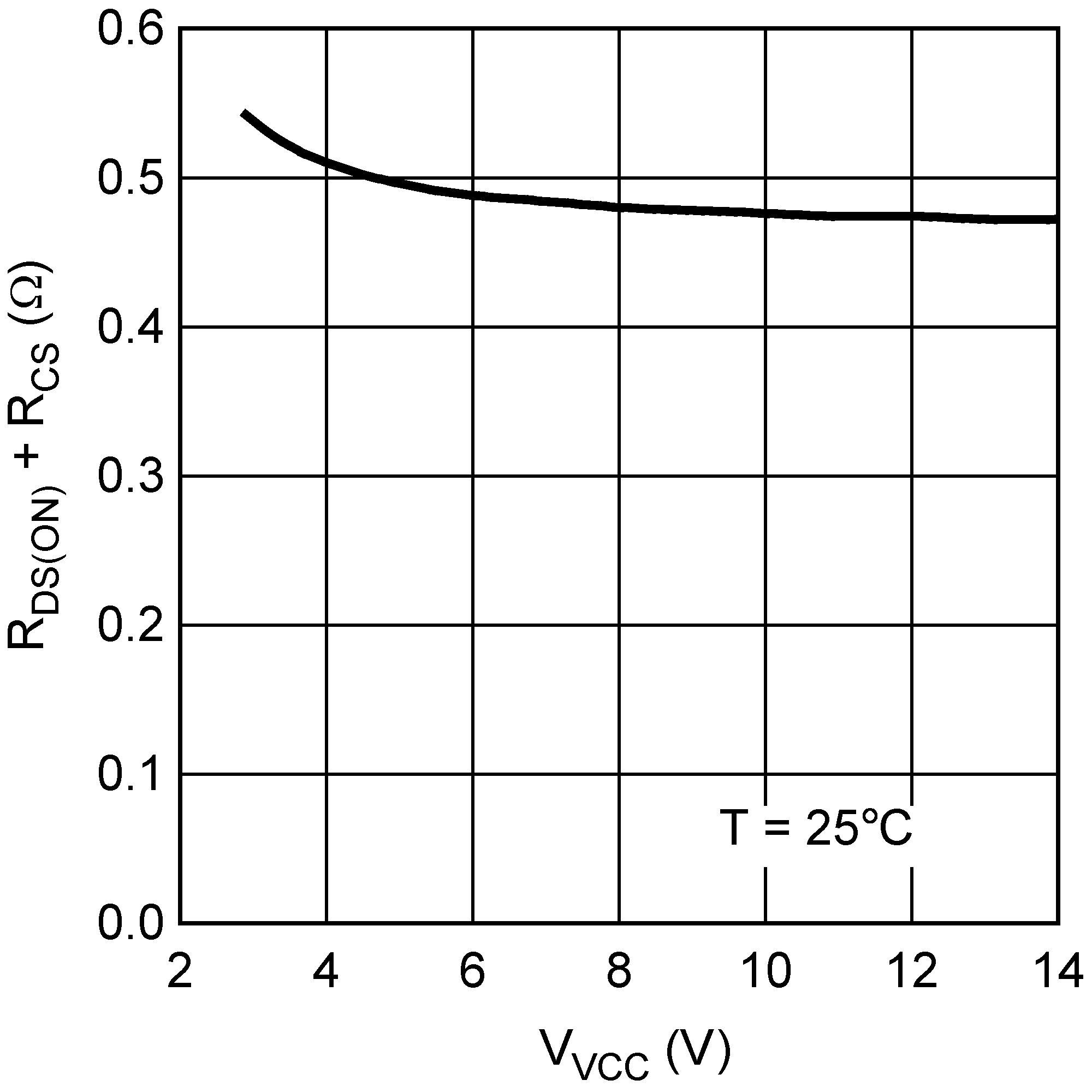
LM5001 LM5001-Q1 20215722.png
Figure 5. RDS(ON) vs VCC
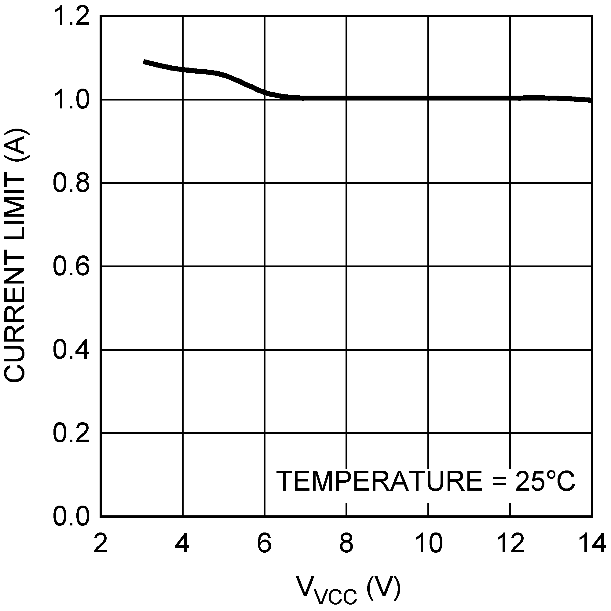
LM5001 LM5001-Q1 20215724.png
Figure 7. ILIM vs VCC
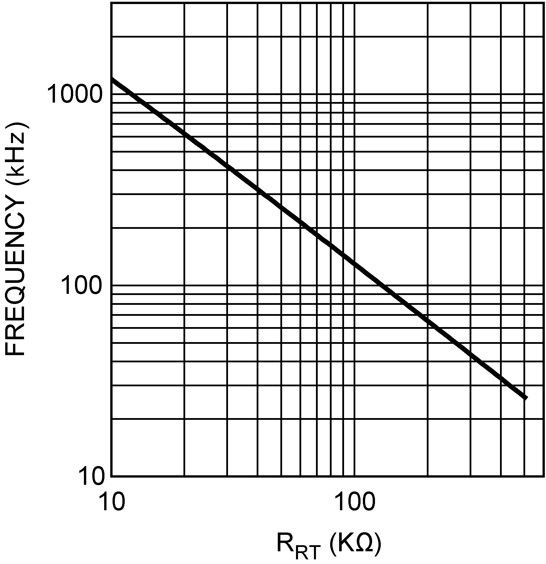
LM5001 LM5001-Q1 20215726.png
Figure 9. FSW vs RRT
LM5001 LM5001-Q1 20215728.png
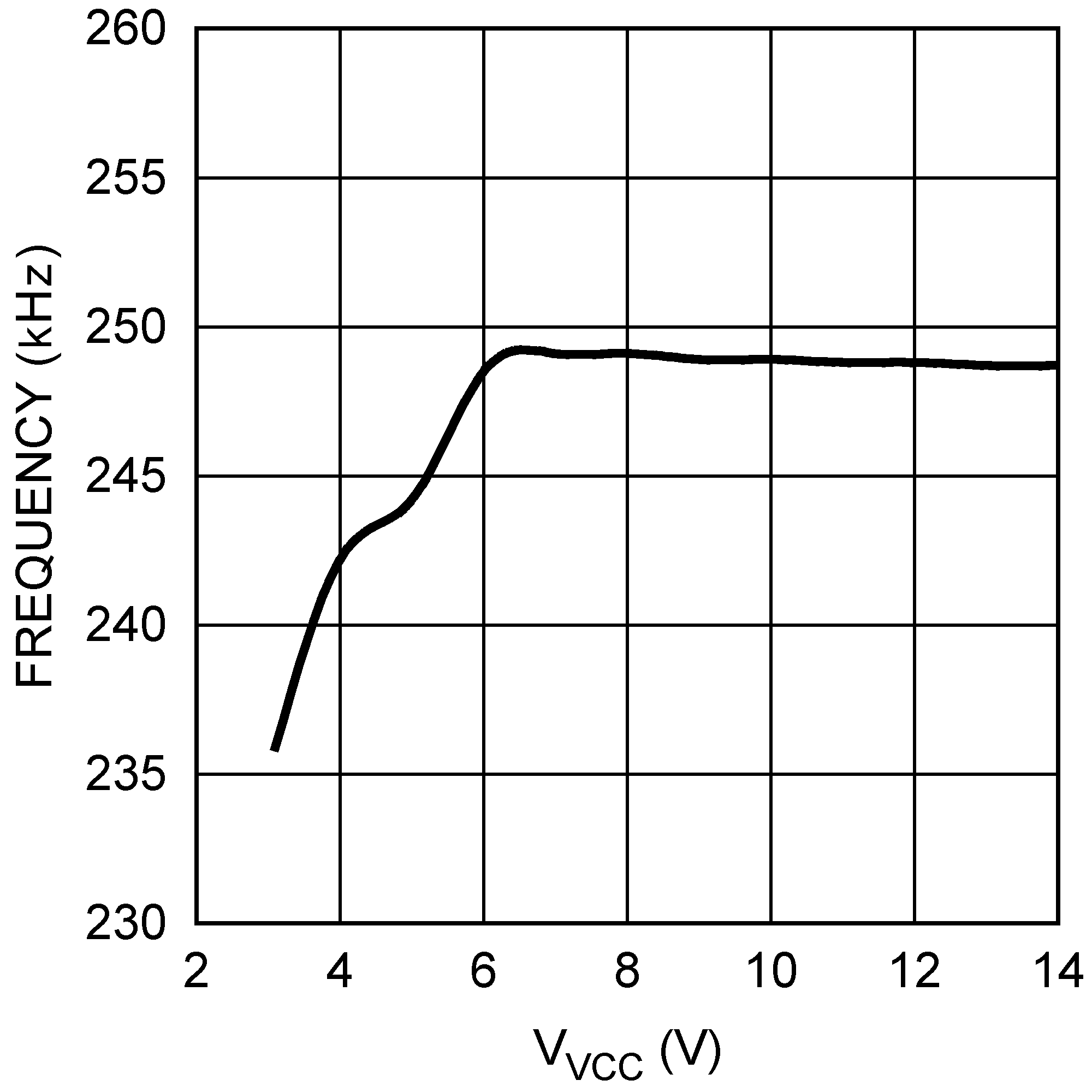
Figure 11. FSW vs VCC
LM5001 LM5001-Q1 20215719.png
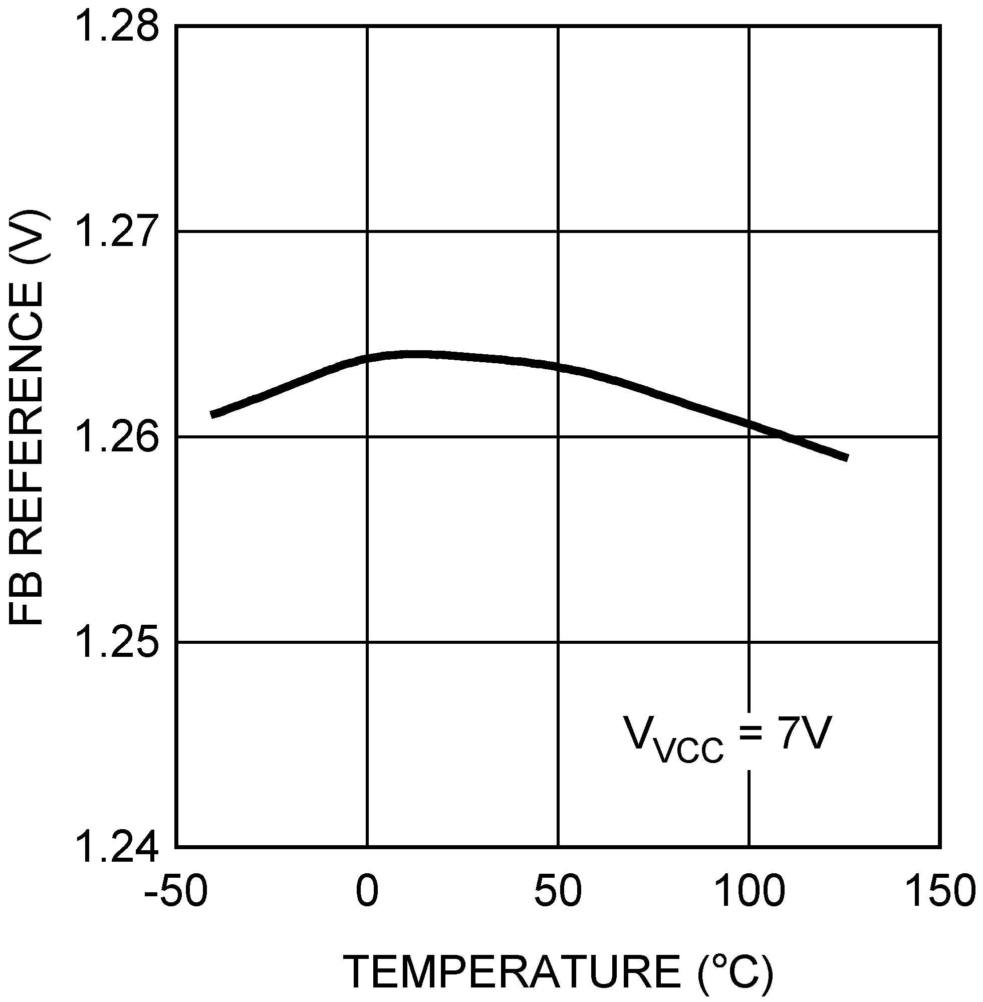
Figure 2. VFB vs Temperature
LM5001 LM5001-Q1 20215721.png
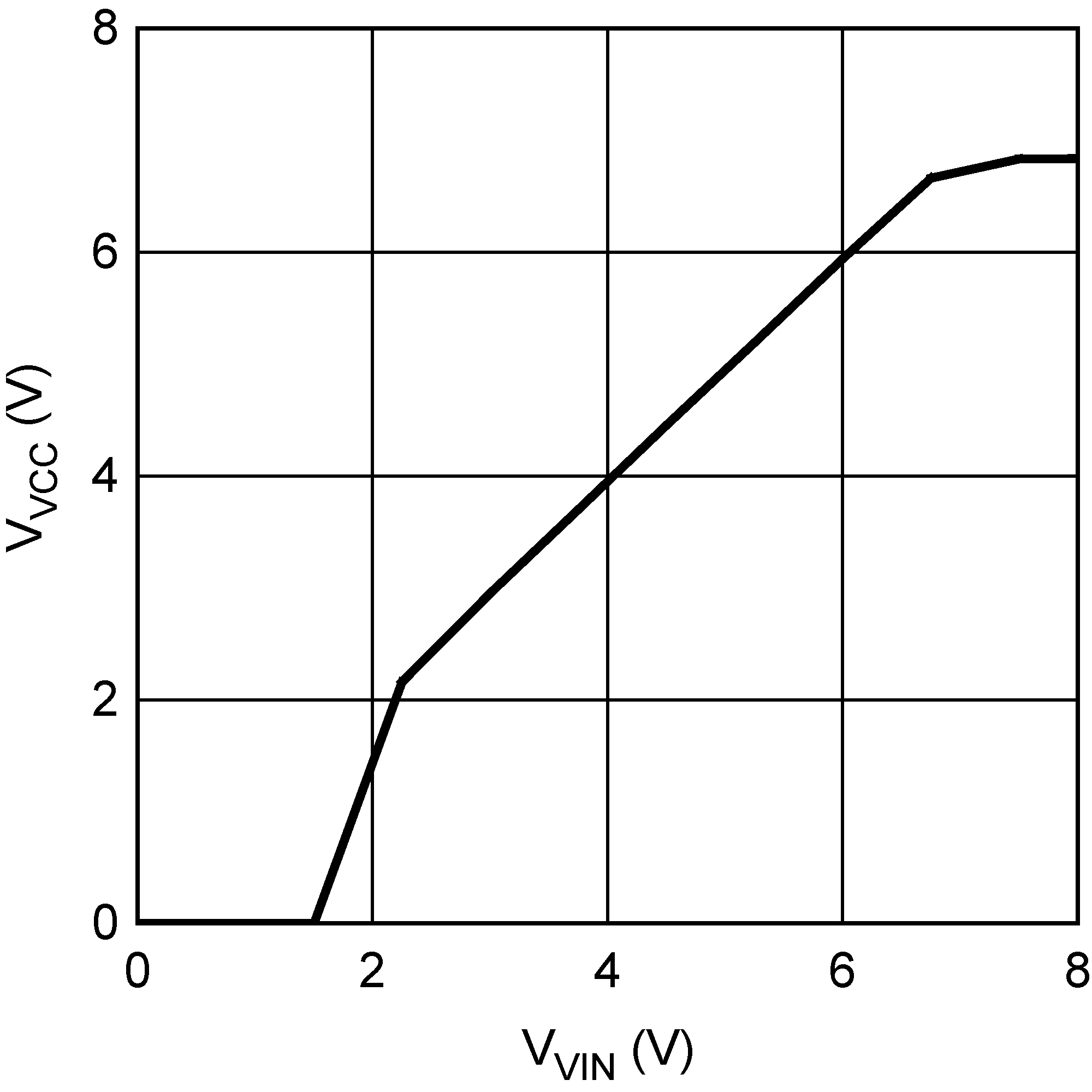
Figure 4. VCC vs VIN
LM5001 LM5001-Q1 20215723.png
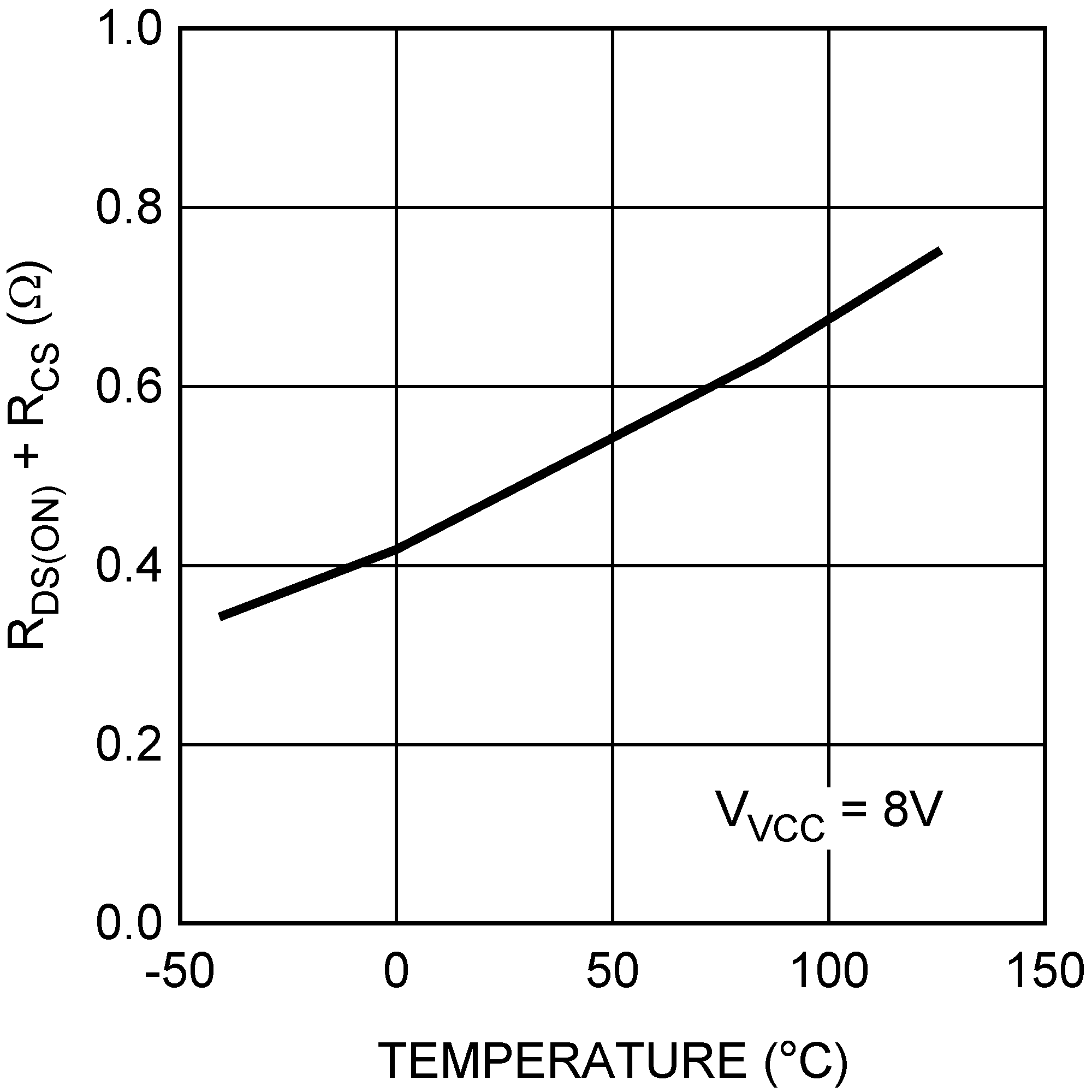
Figure 6. RDS(ON) vs Temperature
LM5001 LM5001-Q1 20215725.png
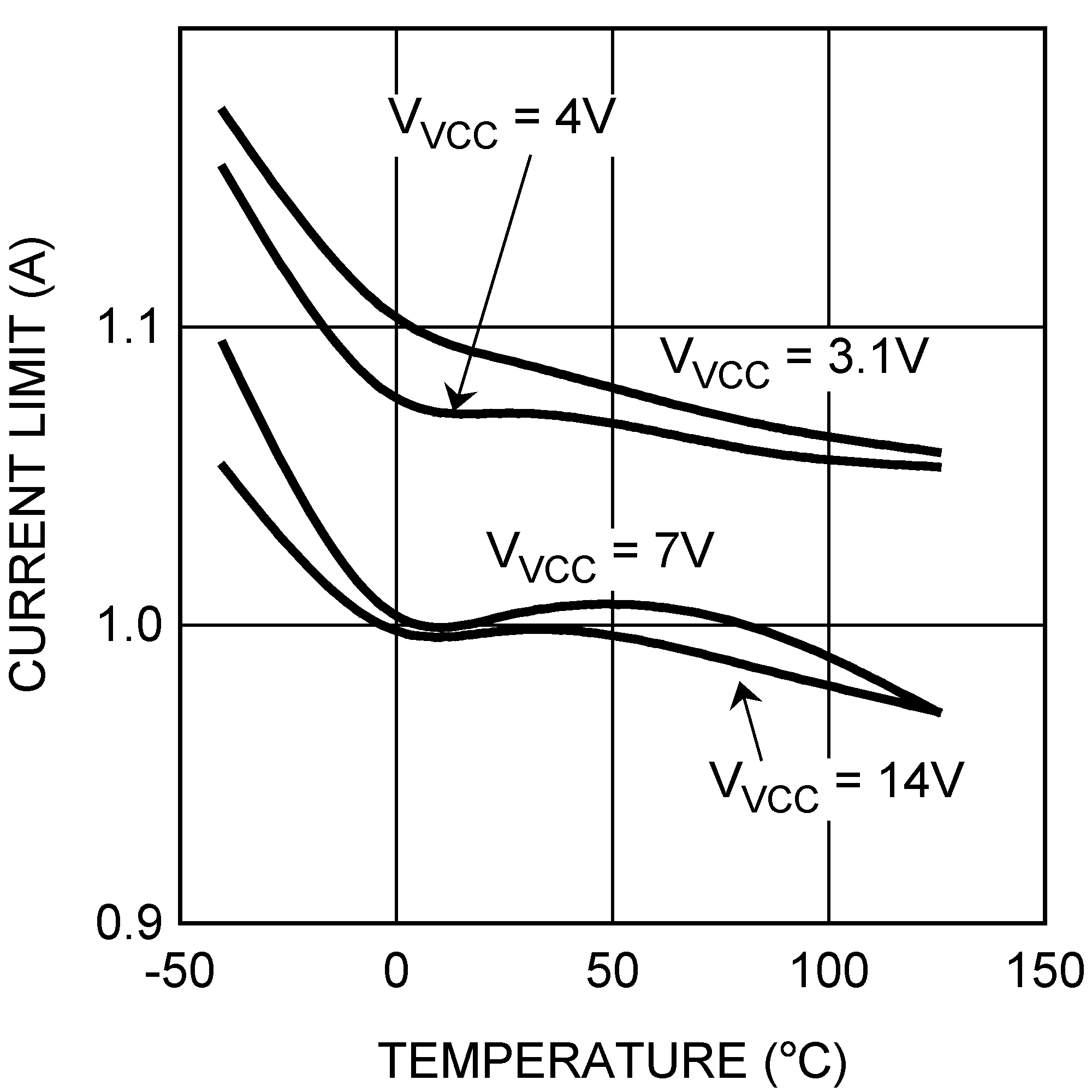
Figure 8. ILIM vs VCC vs Temperature
LM5001 LM5001-Q1 20215727.png
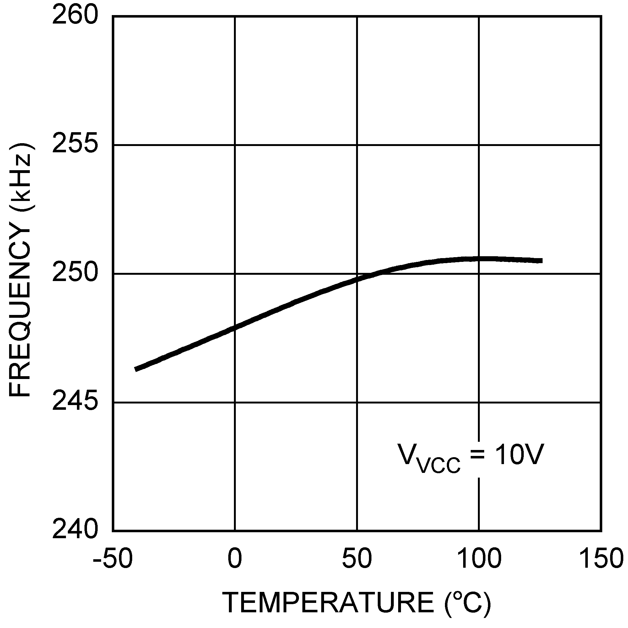
Figure 10. FSW vs Temperature
LM5001 LM5001-Q1 20215729.png
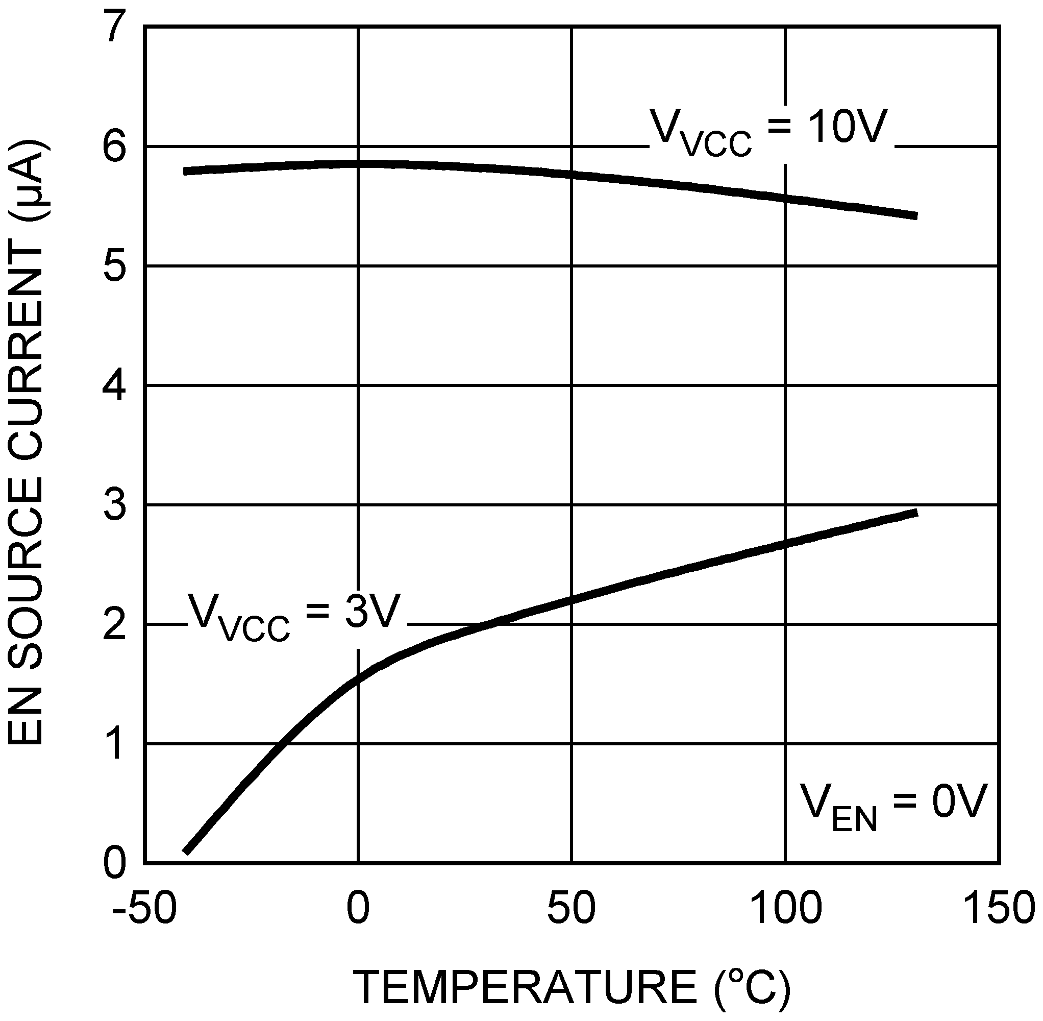
Figure 12. IEN vs VVIN vs Temperature