SNVS402I February 2006 – May 2021 LM5009
PRODUCTION DATA
- 1 Features
- 2 Applications
- 3 Description
- 4 Revision History
- 5 Pin Configuration and Functions
- 6 Specifications
- 7 Detailed Description
-
8 Application and Implementation
- 8.1 Application Information
- 8.2
Typical Application
- 8.2.1 Design Requirements
- 8.2.2
Detailed Design Procedure
- 8.2.2.1 Output Resistor Divider Selection
- 8.2.2.2 Frequency Selection
- 8.2.2.3 Inductor Selection
- 8.2.2.4 VCC and Bootstrap Capacitor
- 8.2.2.5 Output Capacitor Selection
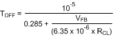
- 8.2.2.6 Current Limit Off-Timer Setting
- 8.2.2.7 Rectifier Diode Selection
- 8.2.2.8 Input Capacitor Selection
- 8.2.2.9 Ripple Configuration
- 8.2.3 Application Curves
- 8.3 Do's and Don'ts
- 9 Power Supply Recommendations
- 10Layout
- 11Device and Documentation Support
- 12Mechanical, Packaging, and Orderable Information
Package Options
Mechanical Data (Package|Pins)
Thermal pad, mechanical data (Package|Pins)
Orderable Information
7.3.6 Current Limit
The LM5009 contains an intelligent current limit off timer. If the current in the buck switch exceeds 0.31 A, then the present cycle is immediately terminated and a non-resettable off timer is initiated. The length of off-time is controlled by an external resistor (RCL) and the FB voltage. When FB = 0 V, a maximum off-time is required and the time is preset to 35 µs. This condition occurs when the output is shorted and during the initial part of start-up. This amount of time ensures safe short-circuit operation up to the maximum input voltage of 95 V. In cases of overload where the FB voltage is above 0 V (not a short-circuit) the current limit off-time is less than 35 µs. Reducing the off-time during less severe overloads reduces the amount of foldback, recovery time, and start-up time. The off-time is calculated from Equation 5:
The current limit sensing circuit is blanked for the first 50 ns to 70 ns of each on-time so it is not falsely tripped by the current surge that occurs at turn-on. The current surge is required by the recirculating diode (D1) for its turn-off recovery.