SNVS402I February 2006 – May 2021 LM5009
PRODUCTION DATA
- 1 Features
- 2 Applications
- 3 Description
- 4 Revision History
- 5 Pin Configuration and Functions
- 6 Specifications
- 7 Detailed Description
-
8 Application and Implementation
- 8.1 Application Information
- 8.2
Typical Application
- 8.2.1 Design Requirements
- 8.2.2
Detailed Design Procedure
- 8.2.2.1 Output Resistor Divider Selection
- 8.2.2.2 Frequency Selection
- 8.2.2.3 Inductor Selection
- 8.2.2.4 VCC and Bootstrap Capacitor
- 8.2.2.5 Output Capacitor Selection
- 8.2.2.6 Current Limit Off-Timer Setting
- 8.2.2.7 Rectifier Diode Selection
- 8.2.2.8 Input Capacitor Selection
- 8.2.2.9 Ripple Configuration
- 8.2.3 Application Curves
- 8.3 Do's and Don'ts
- 9 Power Supply Recommendations
- 10Layout
- 11Device and Documentation Support
- 12Mechanical, Packaging, and Orderable Information
Package Options
Mechanical Data (Package|Pins)
Thermal pad, mechanical data (Package|Pins)
Orderable Information
3 Description
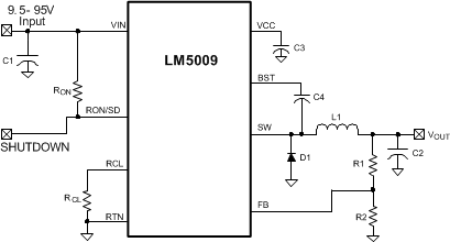
The LM5009 step-down switching regulator features all of the functions needed to implement a low-cost and efficient, buck regulator. This device is capable of driving a 150-mA load current from a 9.5-V to 95-V input source. The switching frequency can exceed 600 kHz, depending on the input and output voltages. The output voltage can be set from 2.5 V to 85 V. This high-voltage regulator contains an N-channel buck switch and an internal startup regulator. The device is easy to implement and is provided in 8-pin VSSOP and thermally-enhanced, 8-pin WSON packages. The regulator operation is based on a control scheme using an on-time inversely proportional to VIN. This feature allows the operating frequency to remain relatively constant over load and input voltage variations. The control scheme requires no loop compensation, resulting in an ultrafast transient response. An intelligent current limit is implemented with forced off-time that is inversely proportional to VOUT. This scheme ensures short-circuit protection and provides minimum foldback. Other features include thermal shutdown, VCC undervoltage lockout, gate drive undervoltage lockout, and maximum duty cycle limiter.
The new product LM5163 offers reduced BOM count, reduced solution size, lower operating quiescent current and many other features. Start WEBENCH® design with LM5163.
| PART NUMBER | PACKAGE | BODY SIZE (NOM) |
|---|---|---|
| LM5009 | VSSOP (8) | 3.00 mm × 3.00 mm |
| WSON (8) | 4.00 mm × 4.00 mm |
 Typical Application Circuit