SNVSBP5 April   2022 LM5013-Q1

PRODUCTION DATA  

  1. Features
  2. Applications
  3. Description
  4. Revision History
  5. Pin Configuration and Functions
  6. Specifications
    1. 6.1 Absolute Maximum Ratings
    2. 6.2 ESD Ratings
    3. 6.3 Recommended Operating Conditions
    4. 6.4 Thermal Information
    5. 6.5 Electrical Characteristics
    6. 6.6 Typical Characteristics
  7. Detailed Description
    1. 7.1 Overview
    2. 7.2 Functional Block Diagram
    3. 7.3 Feature Description
      1. 7.3.1  Control Architecture
      2. 7.3.2  Internal VCC Regulator and Bootstrap Capacitor
      3. 7.3.3  Regulation Comparator
      4. 7.3.4  Internal Soft Start
      5. 7.3.5  On-Time Generator
      6. 7.3.6  Current Limit
      7. 7.3.7  N-Channel Buck Switch and Driver
      8. 7.3.8  Schottky Diode Selection
      9. 7.3.9  Enable/Undervoltage Lockout (EN/UVLO)
      10. 7.3.10 Power Good (PGOOD)
      11. 7.3.11 Thermal Protection
    4. 7.4 Device Functional Modes
      1. 7.4.1 Shutdown Mode
      2. 7.4.2 Standby Mode
      3. 7.4.3 Active Mode
      4. 7.4.4 Sleep Mode
  8. Application and Implementation
    1. 8.1 Application Information
    2. 8.2 Typical Application
      1. 8.2.1 Design Requirements
      2. 8.2.2 Detailed Design Procedure
        1. 8.2.2.1 Custom Design With WEBENCH® Tools
        2. 8.2.2.2 Switching Frequency (RRON)
        3. 8.2.2.3 Buck Inductor (LO)
        4. 8.2.2.4 Schottky Diode (DSW)
        5. 8.2.2.5 Output Capacitor (COUT)
        6. 8.2.2.6 Input Capacitor (CIN)
        7. 8.2.2.7 Type 3 Ripple Network
      3. 8.2.3 Application Curves
  9. Power Supply Recommendations
  10. 10Layout
    1. 10.1 Layout Guidelines
      1. 10.1.1 Compact PCB Layout for EMI Reduction
      2. 10.1.2 Feedback Resistors
    2. 10.2 Layout Example
      1. 10.2.1 Thermal Considerations
  11. 11Device and Documentation Support
    1. 11.1 Device Support
      1. 11.1.1 Third-Party Products Disclaimer
      2. 11.1.2 Development Support
        1. 11.1.2.1 Custom Design With WEBENCH® Tools
    2. 11.2 Documentation Support
      1. 11.2.1 Related Documentation
    3. 11.3 Receiving Notification of Documentation Updates
    4. 11.4 Support Resources
    5. 11.5 Trademarks
    6. 11.6 Electrostatic Discharge Caution
    7. 11.7 Glossary
  12. 12Mechanical, Packaging, and Orderable Information

Package Options

Mechanical Data (Package|Pins)
Thermal pad, mechanical data (Package|Pins)
Orderable Information

On-Time Generator

The on time of the LM5013-Q1 high-side FET is determined by the RRON resistor and is inversely proportional to the input voltage, VIN. The inverse relationship with VIN results in a nearly constant frequency as VIN is varied. Use Equation 3 to calculate the on time.

Equation 3. GUID-C5F94C2C-3C9A-4E38-A971-9F6C3DF5AA9D-low.gif

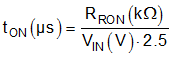
Use Equation 4 to determine the RRON resistor to set a specific switching frequency in CCM.

Equation 4. GUID-08230912-1499-4274-B350-60FFB99B35F1-low.gif

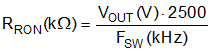
Select RRON for a minimum on time (at maximum VIN) greater than 50 ns for proper operation. In addition to this minimum on time, the maximum frequency for this device is limited to 1 MHz.