SNVS961E APRIL   2013  – January 2016 LM5023

PRODUCTION DATA.  

  1. Features
  2. Applications
  3. Description
  4. Revision History
  5. Pin Configuration and Functions
  6. Specifications
    1. 6.1 Absolute Maximum Ratings
    2. 6.2 ESD Ratings
    3. 6.3 Recommended Operating Conditions
    4. 6.4 Thermal Information
    5. 6.5 Electrical Characteristics
    6. 6.6 Typical Characteristics
  7. Detailed Description
    1. 7.1 Overview
    2. 7.2 Functional Block Diagram
    3. 7.3 Feature Description
      1. 7.3.1 Detailed Pin Description
        1. 7.3.1.1 QR Pin
        2. 7.3.1.2 VSD Pin
        3. 7.3.1.3 SS Pin
        4. 7.3.1.4 COMP Pin
        5. 7.3.1.5 CS Pin
        6. 7.3.1.6 GND Pin
        7. 7.3.1.7 OUT Pin
        8. 7.3.1.8 VCC Pin
      2. 7.3.2 Start-Up
      3. 7.3.3 Quasi-Resonant Operation
      4. 7.3.4 Quasi-Resonant Operating Frequency
      5. 7.3.5 PWM Comparator
      6. 7.3.6 Soft-Start
      7. 7.3.7 Gate Driver
        1. 7.3.7.1 Skip-Cycle Operation
      8. 7.3.8 Current Limit and Current Sense
    4. 7.4 Device Functional Modes
  8. Application and Implementation
    1. 8.1 Application Information
    2. 8.2 Typical Application
      1. 8.2.1 Design Requirements
      2. 8.2.2 Detailed Design Procedure
        1. 8.2.2.1 Custom Design with WEBENCH Tools
        2. 8.2.2.2 Line Current-Limit Feedforward
          1. 8.2.2.2.1 Overvoltage Protection
        3. 8.2.2.3 Valley Switching
        4. 8.2.2.4 Hiccup Mode
      3. 8.2.3 Application Curves
  9. Power Supply Recommendations
  10. 10Layout
    1. 10.1 Layout Guidelines
    2. 10.2 Layout Example
  11. 11Device and Documentation Support
    1. 11.1 Custom Design with WEBENCH Tools
    2. 11.2 Receiving Notification of Documentation Updates
    3. 11.3 Community Resources
    4. 11.4 Trademarks
    5. 11.5 Electrostatic Discharge Caution
    6. 11.6 Glossary
  12. 12Mechanical, Packaging, and Orderable Information

Package Options

Mechanical Data (Package|Pins)
Thermal pad, mechanical data (Package|Pins)
Orderable Information

10 Layout

10.1 Layout Guidelines

TI recommends all high-current loops be kept as short as possible. Keep all high-current and high-frequency traces away from other traces in the design. If necessary, high-frequency and high-current traces should be perpendicular to signal traces, not parallel to them. It is good practice to shield signal traces with ground traces to help reduce noise pick up. The ground reference for components connected to the signal pins should be a kelvin connection to the VCC bypass capacitor and GND pin. Always consider appropriate clearances between high-voltage nets and low-voltage nets.

10.2 Layout Example
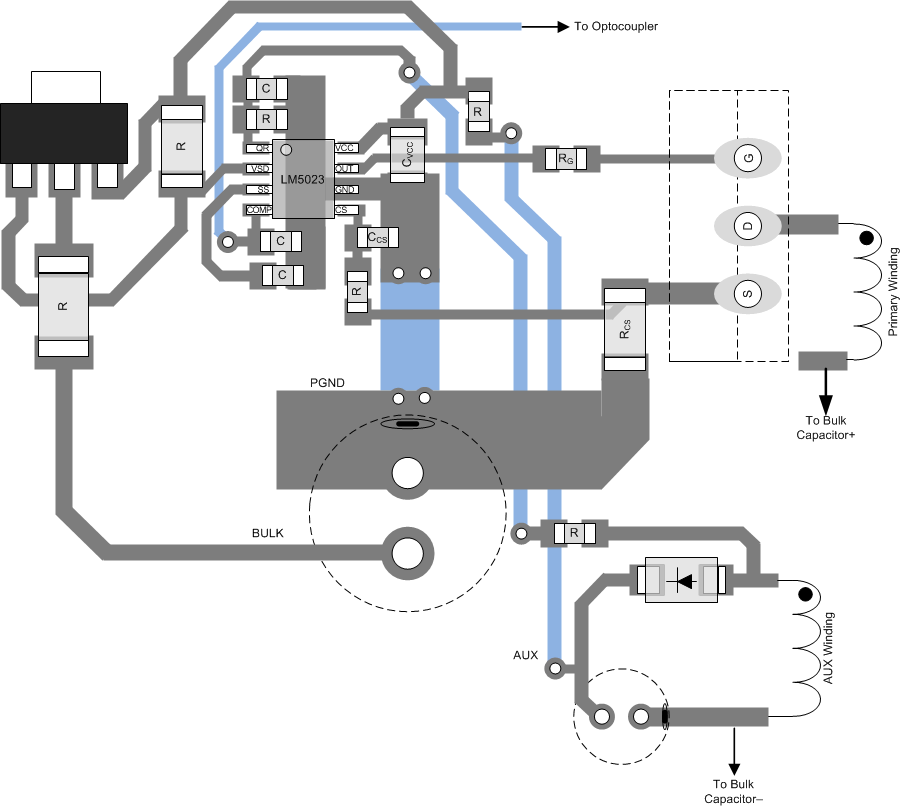
LM5023 layout_snvs961.gif Figure 24. LM5023 Layout Example