SNVS628H October 2009 – December 2019 LM5060
PRODUCTION DATA.
- 1 Features
- 2 Applications
- 3 Description
- 4 Revision History
- 5 Pin Configuration and Functions
- 6 Specifications
- 7 Detailed Description
-
8 Application and Implementation
- 8.1 Application Information
- 8.2
Typical Applications
- 8.2.1
Example Number 1: LM5060EVAL Design
- 8.2.1.1 Design Requirements
- 8.2.1.2
Detailed Design Procedure
- 8.2.1.2.1 VDS Fault Detection and Selecting Sense Pin Resistor RS
- 8.2.1.2.2 Turn-On Time
- 8.2.1.2.3 Fault Detection Delay Time
- 8.2.1.2.4 MOSFET Selection
- 8.2.1.2.5 Input and Output Capacitors
- 8.2.1.2.6 UVLO, OVP
- 8.2.1.2.7 POWER GOOD Indicator
- 8.2.1.2.8 Input Bypass Capacitor
- 8.2.1.2.9 Large Load Capacitance
- 8.2.1.3 Application Curves
- 8.2.2 Example Number 2: Reverse Polarity Protection With Diodes
- 8.2.3 Example Number 3: Reverse Polarity Protection With Resistor
- 8.2.1
Example Number 1: LM5060EVAL Design
- 9 Power Supply Recommendations
- 10Layout
- 11Device and Documentation Support
- 12Mechanical, Packaging, and Orderable Information
Package Options
Mechanical Data (Package|Pins)
- DGS|10
Thermal pad, mechanical data (Package|Pins)
Orderable Information
8.2.3.2.1 Reverse Polarity Protection With a Resistor
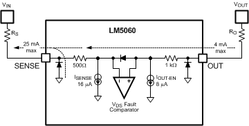
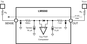
An alternative to using external diodes to protect the LM5060 OUT pin in the reverse polarity input condition is a resistor in series with the OUT pin. Adding an OUT pin resistor may require modification of the resistor in series with the SENSE pin. A resistor in series with the OUT pin will limit the current through the internal zener diode between OUT and GATE as well as through the diode between OUT and SENSE. The value of these resistors should be calculated to limit the current through the diode across the input terminals of the VDS fault comparator to be no more than 4 mA. Figure 42 shows the internal circuitry relevant for calculating the values of the resistor RO in the OUT path to limit the current into the OUT pin to 4 mA.
 Figure 42. Current Limiting Resistor for Negative SENSE Condition
 When calculating the minimum RO resistor required to limit the current into the OUT pin, the internal current sources of 8 µA and 16 µA may be neglected. The following formulas can be used to calculate the resistor value RO(MIN) which is necessary to keep the IO current to less than 4 mA.
Case A is for situations where VOUT > VIN and reverse polarity situation is present (see Figure 42). VIN is negative, but the voltage at the SENSE pin can roughly be assumed to be 0.0 V due to the internal diode from the SENSE pin to GND.

In this case, VIN also has to be limited to a negative voltage so that reverse current through the SENSE pin does not exceed 25 mA.

 Figure 43. Current Limiting Resistor in the OUT Path for OUT > SENSE Condition
 Case B is for situations where VOUT > VIN and there is no reverse polarity situation present (see Figure 43). VIN is positive and VOUT is also positive, but VOUT is higher than VIN:

In this case the voltage on the SENSE pin should not exceed 65 V.
Case C is for situations where VOUT < VIN and both VIN and VOUT are positive as well. In such cases there is no risk of excessive OUT pin current. No current limiting resistors are necessary. Both the SENSE and OUT voltages should be limited to less than 65 V.
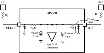
 Figure 44. Current Limiting Resistor for Negative OUT Conditions
 Case D for situations where VOUT < VIN, while VOUT is negative and VIN is positive (see Figure 44). RO needs to be selected to protect the OUT pin from currents exceeding 25 mA.
