SNVS300H July 2004 – September 2016 LM5111
PRODUCTION DATA.
- 1 Features
- 2 Applications
- 3 Description
- 4 Revision History
- 5 Device Options
- 6 Pin Configuration and Functions
- 7 Specifications
- 8 Detailed Description
- 9 Application and Implementation
- 10Power Supply Recommendations
- 11Layout
- 12Device and Documentation Support
- 13Mechanical, Packaging, and Orderable Information
Package Options
Mechanical Data (Package|Pins)
Thermal pad, mechanical data (Package|Pins)
- DGN|8
Orderable Information
8 Detailed Description
8.1 Overview
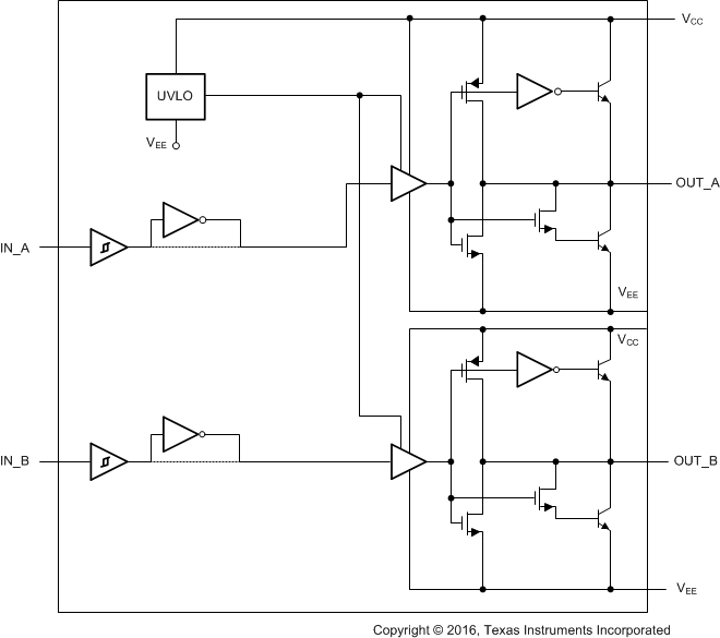
LM5111 dual gate driver consists of two independent and identical driver channels with TTL compatible logic inputs and high current totem-pole outputs that source or sink current to drive MOSFET gates. The driver output consist of a compound structure with MOS and bipolar transistor operating in parallel to optimize current capability over a wide output voltage and operating temperature range. The bipolar device provides high peak current at the critical threshold region of the MOSFET VGS while the MOS devices provide rail-to-rail output swing. The totem pole output drives the MOSFET gate between the gate drive supply voltage VCC and the power ground potential at the VEE pin.
The control inputs of the drivers are high impedance CMOS buffers with TTL compatible threshold voltages. The LM5111 pinout was designed for compatibility with industry standard gate drivers in single supply gate driver applications.
The input stage of each driver should be driven by a signal with a short rise and fall time. Slow rising and falling input signals, although not harmful to the driver, may result in the output switching repeatedly at a high frequency.
8.2 Functional Block Diagram

8.3 Feature Description
8.3.1 Undervoltage Lockout
An undervoltage lockout (UVLO) circuit is included in the LM5111, which senses the voltage difference between VCC and the chip ground pin, VEE. When the VCC to VEE voltage difference falls below 2.8 V both driver channels are disabled. The UVLO hysteresis prevents chattering during brown-out conditions and the driver resumes normal operation when the VCC to VEE differential voltage exceeds approximately 3 V.
The LM5111-1, -2, and -3 devices hold both outputs in the low state in the UVLO condition. The LM5111-4 is distinguished from the LM5111-3 by the active high output state of OUT_A during UVLO. When VCC is less than the UVLO threshold voltage, OUT_A of the LM5111-4 will be locked in the high state while OUT_B will be disabled in the low state. This configuration allows the LM5111-4 to drive a PFET through OUT_A and an NFET through OUT_B with both FETs safely turned off during UVLO.
8.3.2 Output Stage
The two driver channels of the LM5111 are designed as identical cells. Transistor matching inherent to integrated circuit manufacturing ensures that the AC and DC peformance of the channels are nearly identical. Closely matched propagation delays allow the dual driver to be operated as a single with inputs and output pins connected. The drive current capability in parallel operation is precisely 2× the drive of an individual channel. Small differences in switching speed between the driver channels will produce a transient current (shoot-through) in the output stage when two output pins are connected to drive a single load. Differences in input thresholds between the driver channels will also produce a transient current (shoot-through) in the output stage. Fast transition input signals are especially important while operating in a parallel configuration. The efficiency loss for parallel operation has been characterized at various loads, supply voltages and operating frequencies. The power dissipation in the LM5111 increases be less than 1% relative to the dual driver configuration when operated as a single driver with inputs/ outputs connected.
8.4 Device Functional Modes
Table 2. Input/output Logic Table
| LM5111-1M | LM5111-2M | LM5111-3M/LM5111-4M | |||||||||
|---|---|---|---|---|---|---|---|---|---|---|---|
| IN A | IN B | OUT A | OUT B | IN A | IN B | OUT A | OUT B | IN A | IN B | OUT A | OUT B |
| L | L | L | L | L | L | H | H | L | L | H | L |
| L | H | L | H | L | H | H | L | L | H | H | H |
| H | L | H | L | H | L | L | H | H | L | L | L |
| H | H | H | H | H | H | L | L | H | H | L | H |
| In UVLO | L | L | In UVLO | L | L | In UVLO | L/H | L/L | |||