SNVSA02A January 2016 – December 2016 LM5140-Q1
PRODUCTION DATA.
- 1 Features
- 2 Applications
- 3 Description
- 4 Revision History
- 5 Pin Configuration and Functions
- 6 Specifications
-
7 Detailed Description
- 7.1 Overview
- 7.2 Functional Block Diagram
- 7.3
Feature Description
- 7.3.1 High Voltage Start-up Regulator
- 7.3.2 VCC Regulator
- 7.3.3 Oscillator
- 7.3.4 SYNIN and SYNOUT
- 7.3.5 Enable
- 7.3.6 Power Good
- 7.3.7 Output Voltage
- 7.3.8 Minimum Output Voltage Adjustment
- 7.3.9 Current Sense
- 7.3.10 DCR Current Sensing
- 7.3.11 Error Amplifier and PWM Comparator
- 7.3.12 Slope Compensation
- 7.4 Device Functional Modes
- 8 Application and Implementation
- 9 Power Supply Recommendations
- 10Layout
- 11Device and Documentation Support
- 12Mechanical, Packaging, and Orderable Information
Package Options
Mechanical Data (Package|Pins)
- RWG|40
Thermal pad, mechanical data (Package|Pins)
Orderable Information
8 Application and Implementation
NOTE
Information in the following applications sections is not part of the TI component specification, and TI does not warrant its accuracy or completeness. TI’s customers are responsible for determining suitability of components for their purposes. Customers should validate and test their design implementation to confirm system functionality.
8.1 Application Information
The LM5140-Q1 is a synchronous buck controller used to convert a higher input voltage to two lower output voltages. The following design procedure can be used to select external component values. Alternately, the WEBENCH® software may be used to generate a complete design. The WEBENCH software uses an iterative design procedure and accesses a comprehensive database of components when generating a design. This section presents a simplified discussion of the design process. In addition to the WEBENCH software the LM5140ADESIGN-CALC.XIXS quick start Excel calculator is available at www.ti.com.
8.2 Typical Application
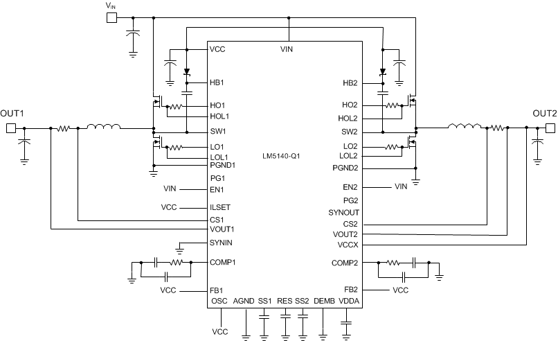 Figure 31. 12-V to 3.3-V and 5-V Converter
8.2.1 Design Requirements
For this design example, the intended input, output and performance parameters are shown in Table 1.
Table 1. Design Parameters
| DESIGN PARAMETER | EXAMPLE VALUE |
|---|---|
| Input voltage range (steady-state) | 8 V to 18 V |
| Transient | 42 V |
| Cold crank | 3.8 V |
| Output voltage | 3.3 V |
| Output current | 6 A |
| Operating frequency | 2.2 MHz |
| Output voltage regulation | ± 1% |
| Standby current, one output enabled, no-load | < 35 µA |
| Shutdown current | 9 µA |
8.2.2 Detailed Design Procedure
- Buck Inductor calculation
- Peak inductor current calculation
- Current Sense resistor
- Output capacitor
- Input filter design
- MOSFET selection
- Control Loop design
8.2.2.1 Inductor Calculation
For peak current mode control, sub-harmonic oscillation occurs with a duty cycle greater than 50% and is characterized by alternating wide and narrow pulses at the SW pin. By adding a slope compensating ramp equal to at least one-half the inductor current down-slope, any tendency toward sub-harmonic oscillation is damped within one switching cycle. For design simplification, the LM5140-Q1 has an internal slope compensation ramp added to the current sense signal.
For the slope compensation ramp to dampen sub-harmonic oscillation, the inductor value should be calculated based on the following guidelines (Equation 14 assumes an inductor ripple current 30%):

- Lower inductor values increase the peak-to-peak inductor current, which minimizes size and cost and improves transient response at the expense of reduced efficiency due to higher peak currents.
- Higher inductance values decrease the peak-to-peak inductor current, which increases efficiency by reducing the RMS current but requires larger output capacitors to meet load-transient specifications.

A standard inductor value of 1.5 µH is selected.


The maximum peak-to-peak inductor current is calculated in Equation 18 through Equation 21:


8.2.2.2 Current Sense Resistor
When calculating the current sense resistor, the maximum output current capability (IOUTMAX) must be at least 20% higher than the required full load current to account for tolerances, ripple current, and load transients. For this example, 120% of the 6.41-A peak inductor current calculated in the previous section (Ipk) is 7.69 A. The current sense resistor value can be calculated using Equation 22 and Equation 23:


where
- VCS is the 73 mV current limit threshold.
The Rsense value selected is 9 mΩ
Carefully observe the PCB layout guidelines to ensure that noise and DC errors do not corrupt the differential current sense signals between the CS and VOUT pins. Place the sense resistor close to the devices with short, direct traces, creating Kelvin-sense connections between the current-sense resistor and the LM5140-Q1.
The propagation delays through the current limit comparator, logic, and external MOSFET gate drivers allow the peak current to increase above the calculated current limit threshold. For a total propogation delay of tdlyTOTAL, the worst case peak current through the inductor with the output is shorted can be calculated from Equation 24:

From the Electrical Characteristics, tdlyTOTAL 40 ns (see Equation 25)

Once the peak current and the inductance parameters are known, the inductor can be chosen. An inductor with a saturation current greater than Ipkshortckt (8.59 Apk) should be selected.
8.2.2.3 Output Capacitor
In a switch mode power supply, the minimum output capacitance is typically selected based on the capacitor ripple current rating and the load transient requirements. The output capacitor must be large enough to absorb the inductor energy and limit over voltage when transitioning from full-load to no-load, and to limit the output voltage undershoot during no-load to full load transients. The worst-case load transient from zero to full load occurs when the input voltage is at the maximum value and a current switching cycle has just finished. The total output voltage drop VOUTUV is the sum of the voltage drop while the inductor is ramping up to support the full load and the voltage drop before the next pulse can occur.
The output capacitance required to maintain the minimum output voltage drop VOUTUV can be calculated in Equation 26 and Equation 27:


where
- ISTEP = 6 A
- VOUTUV = 1% of 3.3 V, or 33 mV
For this example a total of 293 µF of capacitance is used, three 82-µF aluminum capacitors for energy storage and one 47-µF low ESR ceramic capacitor to reduce high frequency noise.
Generally, when sufficient capacitance is used to satisfy the undershoot requirement, the overshoot during a full-load to no-load transient will also be satisfactory. After the output capacitance has been selected, calculate the output ripple current and verify that the ripple current is within the capacitor ripple current ratings.
For this design, the output ripple current is calculated in Equation 28 and Equation 29:


8.2.2.4 Input Filter
A power supply input typically has a relatively high source impedance at the switching frequency. Good-quality input capacitors are necessary to limit the ripple voltage at the VIN pin while supplying most of the switch current during the buck switch on-time. When the buck switch turns on, the current drawn from the input capacitor steps from zero to the valley of the inductor current waveform, then ramps up to the peak value, and then drops to the zero at turnoff.
Average input current can be calculated from the total input power required to support the loads at VOUT1 and VOUT2 in Equation 30:

The efficiency η is assumed to be 83% for this design example, yielding total input power:


The ripple voltage on the input capacitors is reduced significantly with a dual-channel operation because each channel operates 180º out of phase from the other. Capacitors connected in parallel should be evaluated for their RMS current rating. The ripple current splits between the input capacitors based on the relative impedance of the capacitors at the switching frequency.
The input capacitors must be selected with sufficient RMS current rating and the maximum voltage rating. The input ripple current with one channel operating is calculated in Equation 34 and Equation 35:


8.2.2.5 EMI Filter Design
Switching regulators exhibit negative input impedance, which is lowest at the minimum input voltage. An under-damped LC filter exhibits a high output impedance at the resonant frequency of the filter. For stability, the filter output impedance must be less than the absolute value of the converter input impedance.


EMI Filter Design Steps:
- Calculate the required attenuation
- Capacitor CIN represents the existing capacitor at the input of the switching converter
- Filter inductor Lf is usually selected between 1 μH and 10 μH (3.6 µH was used for this application), but it can be smaller to reduce losses in a high current design
- Calculate capacitor Cf
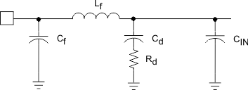 Figure 32. Input EMI Filter
By calculating the first harmonic current from the Fourier series of the input current waveform and multiplying it by the input impedance (the impedance is defined by the existing input capacitor CIN), a formula can be derived to obtain the required attenuation (see Equation 38 and Equation 39):

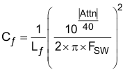
Vmax is the allowed dBμV noise level for the particular EMI standard, CIN is the existing input capacitors of the buck converter. For this application 10 µF was selected. Dmax is the maximum duty cycle. Ipk is the peak inductor current and for filter design purposes, the current at the input can be modeled as a squarewave. The EMI filter capacitor Cf is determined from:
For this application, Cf was chosen to be 1 µF. Adding an input filter to a switching regulator modifies the control-to-output transfer function. The output impedance of the filter must be sufficiently small such that the input filter does not significantly affect the loop gain of the buck converter. The impedance peaks at the filter resonant frequency. The resonant frequency of the filter is given by Equation 42 and Equation 43:


The purpose of Rd is to reduce the peak output impedance of the filter at the resonant frequency. The capacitor Cd blocks the DC component of the input voltage to avoids excessive power dissipation in Rd. The capacitor Cd must have lower impedance than Rd at the resonant frequency with a capacitance value greater than the input capacitor CIN. This prevents the CIN from interfering with the cutoff frequency of the main filter. Added damping is needed when the output impedance is high at the resonant frequency ( Q of filter formed by CIN and Lf is too high): An electrolytic cap Cd can be used as damping device, with the value of Equation 44:

Cd = 4 × 10 µF, a 47-µF capacitor was selected and Rd is chosen using Equation 45 and Equation 46:


8.2.2.6 MOSFET Selection
The LM5140-Q1 gate drivers are powered by the internal 5-V VCC bias regulator. To reduce power dissipation in the controller and improve efficiency, the VCCX pin which must be connected to 5-V output or an external 5-V bias supply. The MOSFETs used with the LM5140 require a logic-level gate threshold with on-resistance specified with VGS = 4.5 V or lower.
The four MOSFETs must be chosen with a VDS rating to withstand the maximum VIN voltage plus supply voltage transients and spikes (ringing). For automotive applications, the maximum VIN occurs during a load dump and the voltage can surge to 42 V under some conditions. A MOSFET with a VDS rating of 60 V would meet most application requirements. The N-channel MOSFETs must be capable of delivering the average load current plus peak ripple current during switching.
The high-side MOSFET losses are associated with the RDS(ON) of the MOSFET and the switching losses.


The losses in the low-side MOSFET include the RDS(ON) losses, the dead time losses, and losses in the MOSFETs internal body diode. The body diode conducts the inductor current during the dead time before the rising edge of the switch node. Minority carriers are injected into and stored in the body diode PN junction. As the high-side FET begins to turn on, a negative current must first flow through the diode to remove the stored charge before the diode can be reverse biased. During this time, the high-side MOSFET drain-source voltage remains at VIN until all the diode minority carriers are removed. Then the diode begins to block negative voltage and the reverse current continues to flow to charge the depletion capacitance of the body diode junction. The total charge required to reverse bias the diode is called reverse-recovery charge Qrr. The power loss in the low-side MOSFET can be calculated from Equation 49 and Equation 50:


where
- tdr and tdf are the switch node voltage rise and fall times (20 ns)
- VDFET the forward voltage drop across the low-side MOSFET internal body diode (0.8 V)
- DQrr the internal body diode reverse recovery charge (105 nC)
- and RDS(ON) the on resistance of the low-side MOSFET ( 26 mΩ at TJ = 125ºC)
Table 2 provides parameters for several MOSFETs that have tested in the LM5140-Q1 evaluation module.
Table 2. EVM MOSFETs
| MANUFACTURER | PART NUMBER | VDS (V) | ID (A) | QgMAX (nC) VGS = 4.5 V |
RDSON MAX (mΩ) VGS = 4.5 |
COSS /MAX | APPLICATION |
|---|---|---|---|---|---|---|---|
| VISHAY | SQJ850EP | 60 | 24 | 30 | 32 | 215 | Automotive High Power |
| VISHAY | SQ7414EN | 60 | 5.6 | 25 | 36 | 175 | Automotive Low Power |
| Texas Instruments | CSD18534Q5A | 60 | 13 | 11.1 | 12.4 | 217 | Industrial |
8.2.2.7 Driver Slew Rate Control
Figure 33 shows the high current driver outputs with independent source and current sink pins for slew rate control. Slew rate control enables the user to adjust the switch node rise and fall times which can reduce the conducted EMI in the FM radio band (30 MHz to 108 MHz). Using the LM5140-Q1 EVM, conducted emission were measured in accordance with CISPR 25. Figure 34 shows the measured results without slew rate control. The conducted EMI results with slew rate control are shown in Figure 35.
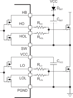 Figure 33. Drivers With Slew Rate Control
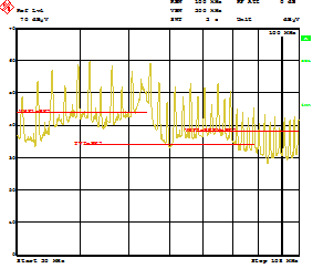 Figure 34. EMI Measurements CISPR 25, No Slew Rate Control
Referring to Figure 34 and Figure 35 a 10-dB reduction in conduction emissions in the FM band is attained by using slew rate control. This can reduce the size and cost of the EMI filters.
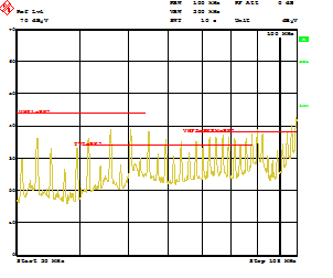 Figure 35. EMI Measurements CISPR 25 With Slew Rate Control
8.2.2.8 Sub-Harmonic Oscillation
For peak current mode control, sub-harmonic oscillation occurs with a duty cycle greater than 50% and is characterized by alternating wide and narrow pulses at the SW pin. By adding a compensating ramp equal to the down-slope of the inductor current, any tendency toward sub-harmonic oscillation is damped within one switching cycle.
In time-domain analysis, the steady-state inductor current starts and ends at the same value during one clock cycle. If the magnitude of the end-of-cycle current error, dI1, caused by an initial perturbation, dI0, is less than the magnitude of dI0 or dI1/dI0 > –1, the perturbation naturally disappears after a few cycles, refer to Figure 36. When dI1/dI0 < –1, the initial perturbation does not disappear resulting in sub-harmonic oscillation in steady-state operation. By choosing K > 1 , sub-harmonic oscillation is avoided.
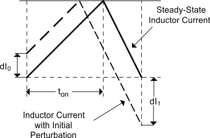 Figure 36. Sub-Harmonic Oscillation

The relationship between Q and K factor is illustrated graphically in Figure 37.
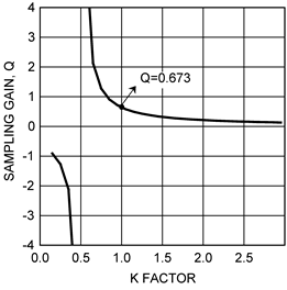 Figure 37. Sampling Gain Q vs K Factor
The minimum value of K is 0.5. This is the same as time domain analysis result. When K < 0.5, the regulator is unstable. High gain peaking at 0.5 results in sub-harmonic oscillation at FSW//2. When K = 1, one-cycle damping is realized and Q is equal to 0.673 at this point. A higher K factor may introduce additional phase shift by moving the sampled gain inductor pole closer to the crossover frequency but helps reduce noise sensitivity in the current loop.
8.2.2.9 Control Loop
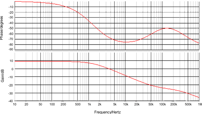
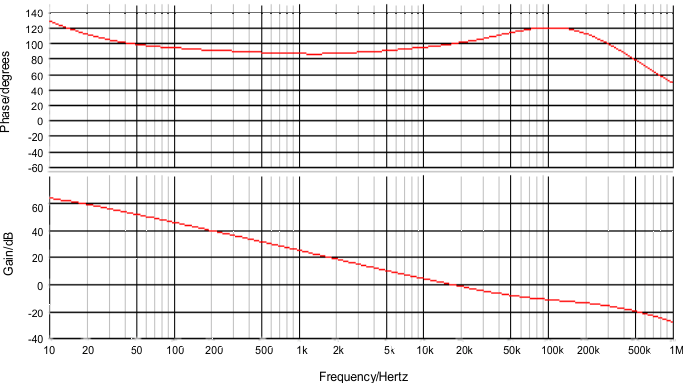
The open-loop gain is defined as the product of modulator and feedback transfer functions. When plotted on a dB scale, the open loop gain is shown as the sum of modulator gain and feedback gain.
DC modulator gain is calculated in Equation 52:

where
- GCS is the current sense amplifier gain (12)
- RLOAD is the load resistance
- RDCR is the dc resistance on the output inductor
- RSENSE is the current sense resistance
The modulator gain plus power stage transfer function with an embedded current loop is shown in Equation 53. The equation included the sample gain at FSW/2 (ωn), which is caused by sampling effect of current mode control.

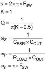
Because the loop cross over frequency is well below sample gain effects, Equation 54 can be simplified as one pole and a one zero system as shown in Equation 55

8.2.2.10 Error Amplifier
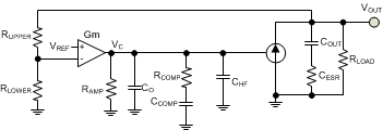
A type ll compensator using an transconductance error amplifier (EA) Gm is shown in Figure 38. The dominant pole of the EA open-loop gain is set by the EA output resistance, RAMP, and effective bandwidth-limiting capacitance, CO as follows:

The EA high frequency pole is neglected in the above expression. The compensator transfer function from the output voltage to COMP, including the gain contribution from the feedback resistor divider network, is calculated in Equation 57:

where
- VREF is the feedback voltage reference (1.2 V)
- Gm is the error amplifier gain transconductance (1200 µS)
- and RAMP is the error amplifier output impedance (2.5 MΩ)


Typically RCOMP <<RAMP and CCOMP>> (CO) so the approximations are valid.
The error amplifier compensation components create a pole at the origin, a zero, and a high frequency pole.
The procedure for choosing compensation components for a stable closed loop is:
- Select the desired open-loop gain crossover frequency (fc); for this application 30 kHz was chosen
- Calculate the RCOMP resistor for the gain crossover frequency at 30 kHz
- Calculate the CCOMP capacitor value to create a zero that cancels the pole ωp.


The value selected for RCOMP is 22.6 kΩ

The value selected for CCOMP is 10 nF


