SNVSA02A January 2016 – December 2016 LM5140-Q1
PRODUCTION DATA.
- 1 Features
- 2 Applications
- 3 Description
- 4 Revision History
- 5 Pin Configuration and Functions
- 6 Specifications
-
7 Detailed Description
- 7.1 Overview
- 7.2 Functional Block Diagram
- 7.3
Feature Description
- 7.3.1 High Voltage Start-up Regulator
- 7.3.2 VCC Regulator
- 7.3.3 Oscillator
- 7.3.4 SYNIN and SYNOUT
- 7.3.5 Enable
- 7.3.6 Power Good
- 7.3.7 Output Voltage
- 7.3.8 Minimum Output Voltage Adjustment
- 7.3.9 Current Sense
- 7.3.10 DCR Current Sensing
- 7.3.11 Error Amplifier and PWM Comparator
- 7.3.12 Slope Compensation
- 7.4 Device Functional Modes
- 8 Application and Implementation
- 9 Power Supply Recommendations
- 10Layout
- 11Device and Documentation Support
- 12Mechanical, Packaging, and Orderable Information
Package Options
Mechanical Data (Package|Pins)
- RWG|40
Thermal pad, mechanical data (Package|Pins)
Orderable Information
7 Detailed Description
7.1 Overview
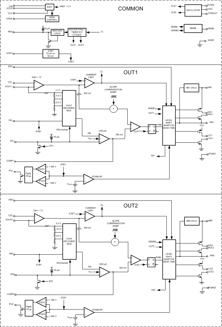
The LM5140-Q1 is a dual-channel switching controller which features all of the functions necessary to implement a high efficiency buck power supply that can operate over a wide input voltage range. The LM5140-Q1 is configured to provide two independent outputs. VOUT1 can be a fixed 3.3 V, 5 V, or adjustable between 1.5 V to 15 V. VOUT2 can be a fixed 5 V, 8 V, or adjustable between 1.5 V to 15 V. This easy to use controller integrates high-side and low-side MOSFET drivers capable of sourcing 3.25 A and sinking 4.25-A peak . The control method is current mode control which provides inherent line feedforward, cycle-by-cycle current limiting, and ease-of-loop compensation. With the OSC pin connected to VDD the default oscillator frequency is 2.2 MHz. With the OSC pin grounded the oscillator frequency is 440 kHz. A synchronization pin allows the LM5140-Q1 to be synchronized to an external clock. Fault protection features include current limiting, thermal shutdown, and remote shutdown capability. The LM5140-Q1 incorporates features that simplify compliance with the CISPR and Automotive EMI requirements. The LM5140-Q1 gate drivers provide adaptive slew rate control and interleaved operation (180 degree output of phase) of the two controller channels. The 4-pin VQFN package with Wettable Flanks features an exposed pad to aid in thermal dissipation.
7.2 Functional Block Diagram
7.3 Feature Description
7.3.1 High Voltage Start-up Regulator
The LM5140-Q1 contains an internal high voltage VCC bias regulator that provides the bias supply for the PWM controller and the gate drivers for the external MOSFETs. The input pin (VIN) can be connected directly to an input voltage source up to 65 V. The output of the VCC regulator is set to 5 V. When the input voltage is below the VCC set-point level, the VCC output tracks VIN with a small voltage drop.
In high voltage applications, take extra care to ensure the VIN pin does not exceed the absolute maximum voltage rating of 70-V curing line or load transients. Voltage ringing on the VIN pin that exceeds the Absolute Maximum Ratings can damage the IC. Use care during PCB board layout and high quality bypass capacitors to minimize ringing.
7.3.2 VCC Regulator
The VCC regulator output current limit is 150 mA (minimum). At power up, the regulator sources current into the capacitors connected to the VCC pin. When the voltage on the VCC pin exceeds 3.4 V both output channels are enabled (if EN1 and EN2 are connected to a voltage source > 2.4 V) and the soft-start sequence begins. Both channels remain active unless the voltage on the VCC pin falls below the VCCUVLO threshold, of 3.2 V (typical) or the enable pins are switched to a low state. The LM5140-Q1 has two VCC pins; these pin must be connected together on the PCB. TI recommends that the VCC capacitor be split between the two VCC pins and connected to the respective PGND pins. The recommended range for the VCC capacitor is from 2.2 µF to 5 µF total.
An internal 5-V linear regulator generates the VDDA bias supply. Bypass VDDA with a 100-nF or greater ceramic capacitor to ensure a low noise internal bias rail. Normally VDDA is 5 V, but there are two operating conditions where it regulates at 3.3 V. The first is in skip cycle mode with VOUT1 set to 3.3 V, and VOUT2 is disabled. The second is in a cold crank start-up where VIN is 3.8 V and VOUT1 is 3.3 V.
Internal power dissipation in the VCC Regulator can be minimized by connecting the VCCX pin to a 5-V output at VOUT1 or VOUT2 or to an external 5-V supply. If VCCX > 4.5 V, VCCX is internally connected to VCC and the internal VCC regulator is disabled. If VCCX is unused, it must be grounded. Never connect the VCCX pin to a voltage greater than 6.5 V.
7.3.3 Oscillator
The LM5140-Q1 has independent oscillators that generate the clock for each channel and can be programmed to 2.2 MHz or 440 kHz with the OSC pin. With the OSC pin connected to VDDA, both oscillators will be set to 2.2 MHz. With OSC grounded, they will both be set to 440 kHz. The state of the OSC pin is read and latched during VCC power up and thus cannot be changed until VCC drops below the VCCUVLO threshold. CLK1 is the clock for channel 1; CLK2 is for channel 2. CLK1 and CLK2 are 180º out of phase. The rising edge of SYNOUT always corresponds to the rising edge of CLK2 which is 180º out of phase with CLK1.
Under low VIN conditions when either of the high-side buck switch on time exceeds the programmed oscillator period, the LM5140-Q1 will extend the oscillator period of that channel until the PWM latch is reset by the current sense ramp exceeding the controller compensation voltage. In such an event, the oscillators (CLK1 and CLK2) operate independently and asynchronously until both channels can maintain output regulation at the programmed frequency.
The approximate input voltage level where this occurs is in Equation 1:

where
- tp = is the oscillator period, 454 ns (for 2.2 MHz operation)
- ton(max) = 354 ns
For example, if VOUT1 = 3.3 V and VOUT2 = 5 V and VIN drops to 6.41 V (see Equation 2).

In the above example, CLK2 frequency is required to drop to maintain regulation of VOUT2 while CLK1 can remain at the programmed frequency (refer to Figure 19). If VIN continues to drop, both CLK1 and CLK2 frequencies are reduced Figure 20.
 Figure 19. HO1, HO2, and SYNOUT VIN 6.41 V
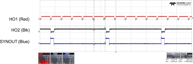 Figure 20. HO1, HO2, SYNOUT VIN 4.2 V
Under high input voltage conditions (VIN > 20 V) when the buck switch on-time of either controller reaches the minimum on-time of 45 ns typical, the LM5140-Q1 reduces the oscillator frequency by skipping clock cycles for the appropriate channel.
Using the same output voltages as in the example above with VIN = 36 V, CLK1 drops to 1.1 MHz and CLK2 is 2.2 MHz, (refer to Figure 21), and SYNOUT is 2.2 MHz.
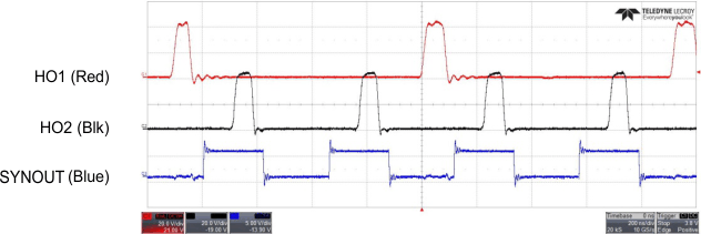 Figure 21. HO1, HO2, and SYNOUT VIN 36 V
7.3.4 SYNIN and SYNOUT
The SYNIN pin can be used to synchronize the LM5140-Q1 to an external clock. The synchronization range when the internal oscillator is set to 440 kHz is 374 kHz minimum to 506 kHz maximum. When the internal oscillator is set to 2.2 MHz, the synchronization range is 1.87 MHz to 2.53 MHz. If the synchronization feature is not being used, the SYNIN pin must be grounded.
CLK1 starts on the rising edge of the external synchronization clock (SYNIN). The HO1 pulse will follow approximately 110 ns after CLK1 due to internal delays (refer to Figure 22). Similarly, CLK2 generates the HO2 pulse after a short delay, and CLK2 is 180º out of phase with CLK1. SYNOUT always corresponds to the rising edge of CLK2.
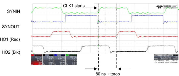 Figure 22. SYNIN and HO1 Timing (2.2 MHz)
Under low VIN conditions when the frequency must be reduced to maintain output voltage regulation, the SYNIN input function adapts as necessary. If VOUT1 can maintain regulation at the SYNIN frequency and VOUT2 cannot, then CLK1 remains synchronized to SYNIN and the CLK2 frequency is reduced (refer to Figure 23). If VOUT1 cannot maintain regulation at the SYNIN frequency, then the SYNIN signal is ignored and channel 1 frequency is reduced to maintain regulation. Channel 2 runs at the frequency determined by OSC pin or lower if required to maintain regulation on VOUT2 (refer to Figure 24).
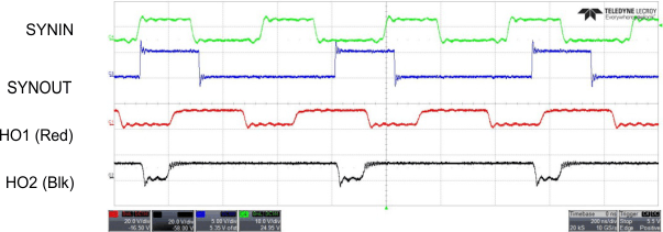 Figure 23. SYNIN (2.2 MHz) VIN 6.41 V
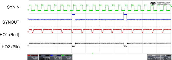 Figure 24. SYNIN (2.2 MHz) VIN 4.2 V
At high VIN when pulse skipping is necessary, HO1 drops to 1.1 MHz and HO2 remains at 2.2 MHz (refer to Figure 25), and SYNOUT is 2.2 MHz.
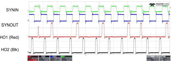 Figure 25. SYNIN (2.2 MHz) VIN 36 V
7.3.5 Enable
The LM5140-Q1 contains two enable inputs, EN1 and EN2. The enable pins allow independent start-up and shutdown control of VOUT1 (EN1) and VOUT2 (EN2). The enable pins can be connected to a voltage as high as 70 V. If the enable input is greater than 2.4 V, the respective controller output is enabled. If the enable pins is pulled below 0.4 V, the respective output will be in shutdown. If both outputs are disabled the LM5140-Q1 is in a low IQ shutdown mode, with 9-µA typical current drawn from the VIN pin. TI does not recommend leaving either of the EN pins floating.
7.3.6 Power Good
The LM5140-Q1 includes output voltage monitoring signals for VOUT1 and VOUT2 to simplify sequencing and supervision. The power good function can be used to enable circuits that are supplied by the corresponding voltage rail or to turn-on sequenced supplies. Each power good output (PG1 and PG2) switches to a high impedance open-drain state when the corresponding output voltage is in regulation. Each output switches low when the corresponding output voltage drops below the lower power good threshold (92% typical) or rises above the upper power good threshold (110% typical). A 25-µs deglitch filter prevents any false tripping of the power good signals due to transients. TI recommends pullup resistors of 10 kΩ (typical) from PG1 and PG2 to the relevant logic rail. PG1 and PG2 are asserted low during soft-start and when the corresponding buck converter is disabled by EN1 or EN2.
7.3.7 Output Voltage
The LM5140-Q1 outputs can be independently configured for one of two fixed output voltages with no external feedback resistors or adjusted to the desired voltage using external resistor dividers. VOUT1 can be configured as a 3.3-V output by connecting the FB1 pin to VDDA, or a 5-V output by connecting the FB1 pin to ground with a maximum resistance of 500 Ω. VOUT2 can be configured as either a 5-V output or 8-V output. For a 5-V output at VOUT2, connect the FB2 pin to VDDA. For a fixed 8-V output at VOUT2 connect FB2 to ground with a maximum resistance of 500 Ω. The FB1 and FB2 connections (either VDDA or GND) are detected during power up. The configuration setting is latched and can not be changed until the LM5140-Q1 is powered down with VCC falling below VCC(UVLO) (3.4 V typical) and then powered up again.
Alternative output voltages can be set external resistive dividers from output to the FB pins. The output voltage adjustment range is between 1.5 V and 15 V. The regulation threshold at the FB pin is 1.2 V (VREF). To calculate RFB1 and RFB2 use Equation 3, refer to Figure 26:

The recommend value for R(FB1) is between 10 kΩ to 20 kΩ.
The Thevenin equivalent impedance of the resistive divider connected to the FB pins must be greater than 5 kΩ for the LM5140-Q1 to detect the divider and set the channel to the adjustable output mode.

If a low IQ mode is required, take care when selecting the external resistors. The extra current drawn from the external divider is added to the LM5140-Q1 I(STANDBY) current (35 µA typical). The divider current reflected to VIN is divided down by the ratio of VOUT/VIN. For example, if VOUT is set to 5.5 V with RFB1 10 kΩ, and RFB2 = 35.8 kΩ (use 35.7 kΩ), the input current at VIN required to supply the current in the feedback resistors is:


VIN = 12 V
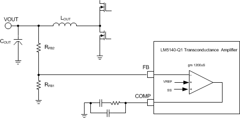 Figure 26. Voltage Feedback
If one output is enabled and the other disabled, VCC output will be in regulation. The HB pin voltage of the disabled channel will charge to VCC through the boot strap diode. As a result, the HO driver bias current (approximately 3 µA) can charge the disabled channel VOUT to approximately 2.2 V. If this is not desired, a load resistor (100 kΩ) can be added to the output that is disabled to maintain a low voltage OFF-state.
7.3.8 Minimum Output Voltage Adjustment
There are two limitations to the minimum output voltage adjustment range: the LM5140-Q1 voltage reference 1.2 V and the minimum switch node pulse width, tSW.
The minimum controllable voltage at the switch node (tSW) limits the voltage conversion ratio (VOUT/VIN). For fixed-frequency PWM operation, the voltage conversion ratio must meet Equation 7:

where
- tSW is 70 ns (typical)
- and Fsw is the switching frequency
If the desired voltage conversion ratio does not meet the above condition, the controller transitions from fixed frequency operation into a pulse skipping mode to maintain regulation of the output voltage.
For example if the desired output voltage is 3.3 V with a VIN of 20 V and operating at 2.2 MHz, the voltage conversion ratio test is in Equation 8:

For Wide VIN applications and lower output voltages, an alternative is to use the LM5140-Q1 with 440-kHz oscillator frequency. Operating at 440 kHz, the limitation with the minimum ton time is less significant. For example, if a 1.8-V output is required with a VIN of 50 V (see Equation 9):

7.3.9 Current Sense
There are two methods to sense the inductor current of the buck converters. The first is using current sense resistor in series with the inductor and the second is to use the DC resistance of the inductor (DCR sensing). Figure 27 illustrates inductor current sensing using a current sense resistor. This configuration continuously monitors the inductor current providing accurate current-limit protection. For the best current-sense accuracy and overcurrent protection, use a low inductance ±1% tolerance current-sense resistor between the inductor and output, with a Kelvin connection to the LM5140-Q1 sense amplifier.
The LM5140-Q1 provides two user selectable current limit levels of 48 mV and 73 mV. If the ILSET pin is connected to VDDA, the current limit threshold is 73 mV. When the ILSET pin is connected to ground, the current limit set point is 48 mV. The ILSET pin is monitored during power up and the setting is latched. To change the setting, VIN power must be removed from the controller allowing the VCC voltage to drop below VCC(UVLO).
If the peak differential current signal sensed from CS to VOUT exceeds the user selectable current limit level of 48 mV or 73 mV, the current limit comparator immediately terminates the HO output for cycle-by-cycle current limiting.

where
- VCS is user selectable threshold of 48 mV or 73 mV.
- IOUTmax is the overcurrent setpoint which is set higher than the maximum load current to avoid tripping the overcurrent comparator during load transients.
- ΔI is the peak-peak inductor current.
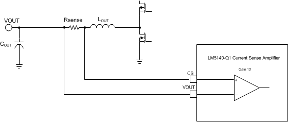 Figure 27. Current Sense
7.3.10 DCR Current Sensing
For high-power applications which do not require high accuracy current-limit protection, DCR sensing may be preferable. This technique provides lossless and continuous monitoring of the output current using an RC sense network in parallel with the inductor. Using an inductor with a low DCR tolerance, the user can achieve a typical current limit accuracy within the range of 10% to 15% at room temperature.
Components RSC and CCS in Figure 28 create a low-pass filter across the inductor to enable differential sensing of the voltage drop across inductor DCR. When RCS × CCS is equal to LOUT/LDCR, the voltage developed across the sense capacitor, CS, is a replica of the inductor DCR voltage waveform. Choose the capacitance of CCS to be greater than 0.1 μF to maintain a low impedance sensing network, thus reducing the susceptibility of noise pickup from the switch node. Carefully observe the PCB layout guidelines to ensure the noise and DC errors do not corrupt the differential current-sense signals applied across the CS and VOUT pins.
The voltage drop across CCS in Equation 11:
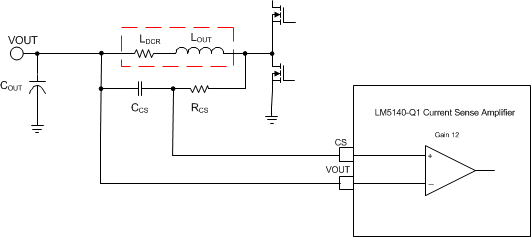 Figure 28. DCR Current Sensing
RCSCCS = LOUT/LDCR → accurate DC and AC current sensing.
If the RC time constant is not equal to the LOUT/LDCR time constant, there is an error.
RCSCCS > LOUT/LDCR → DC level still correct, the AC amplitude is attenuated.
RCSCCS < LOUT/LDCR → DC level still correct, the AC amplitude is amplified.
7.3.11 Error Amplifier and PWM Comparator
Each channel of the LM5140-Q1 has an independent high-gain transconductance amplifier which generates an error current proportional to the difference between the feedback voltage and an internal precision reference (1.2 V). The output of each transconductance amplifier is connected to the COMP pin allowing the user to provide external control loop compensation. Generally for current mode control a type II network is recommended.
7.3.12 Slope Compensation
The LM5140-Q1 provides internal slope compensation to ensure stable operation with duty cycle greater than 50%. To correctly use the internal slope compensation, the inductor value must be calculated based on the following guidelines (Equation 12 assumes an inductor ripple current of 30%):

- Lower inductor values increase the peak-to-peak inductor current, which minimizes size and cost and improves transient response at the cost of reduced efficiency due to higher peak currents.
- Higher inductance values decrease the peak-to-peak inductor current, which increases efficiency by reducing the RMS current at the cost of requiring larger output capacitors to meet load-transient specifications.
7.4 Device Functional Modes
7.4.1 Hiccup Mode Current Limiting
The LM5140-Q1 includes an optional hiccup mode protection function that is enabled when a capacitor is connected to the RES pin. In normal operation the RES capacitor is discharged to ground. If 512 cycles of cycle-by-cycle current limiting occur on a either channel, the SS pin capacitor of that channel is pulled low and the HO and LO outputs are disabled (refer to Figure 29). A 20-μA current source begins to charge the RES capacitor. When the RES pin charges to 1.2 V, the RES pin is pulled low and the SS capacitor begins to charge. The 512 cycle hiccup counter is reset if 4 consecutive switching cycles occur without exceeding the current limit threshold. Separate hiccup counters are provided for each channel, but the RES pin is shared by both channels. One channel can be in the hiccup protection mode while the other operates normally. In the event that both channels are in an overcurrent condition triggering hiccup protection, the last hiccup counter to expire pulls RES low and starts the RES capacitor charging cycle. Both channels then restart together when RES=1.2 V. If RES is connected to VDDA at power up, the hiccup function is disabled for both channels.
The controller is in forced PWM (FPWM) continuous conduciton mode when the DEMB pin is connected to VDDA. In this mode the SS pin is clamped to a level 200 mV above the feedback voltage to the internal error amplifier. This ensures that SS can be pulled low quickly during a brief overcurrent event and prevent overshoot of VOUT when the overcurrent condition is removed.
If DEMB=0 V, the controller operates in diode emulation with light loads (discontinous conduction mode) and the SS pin is allowed to charge to VDDA. This reduces the quiescent current of the LM5140-Q1. If 32 or more cycle-by-cycle current limit events occur, the SS pin is clamped to 200 mV above the feedback voltage to the internal error amplifier until the hiccup counter is reset. Thus, if a momentary overload occurs that causes at least 32 cycles of current limiting, the SS capacitor voltage is slightly higher than the FB voltage and controls VOUT during recovery.
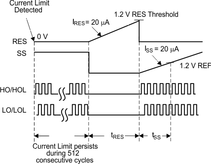 Figure 29. Hiccup Mode
7.4.2 Standby Mode
The LM5140-Q1 operates with peak current mode control such that the feedback compensation voltage is proportional to the peak inductor current. During no-load or light load conditions, the output capacitor discharges very slowly. As a result the compensation voltage does not demand a driver output pulses on a cycle-by-cycle basis. When the LM5140-Q1 controller detects that there have been 16 missing switching cycles, it enters Standby Mode and switches to a low IQ state to reduce the current drawn from VIN. For the LM5140-Q1 to go into a Standby Mode, the controller must be programmed for diode emulation (DEMB pin < 0.4 V). The typical IQ in Standby Mode is 35 µA with VOUT1 regulating at 3.3 V and VOUT2 disabled. With VOUT1 disabled and VOUT2 regulating to 5 V, the Standby Mode current is 42 μA. With both channels in standby mode (VOUT1 = 3.3 V and VOUT2 = 5 V) the VIN current is 75 μA. Using external feedback resistors add additional load to VOUT and significantly increase the Standby Mode VIN current.
7.4.3 Soft Start
The soft-start feature allows the regulator to gradually reach the steady-state operating point, thus reducing start-up stresses and surges. The LM5140-Q1 regulates the FB pin to the SS pin voltage or the internal 1.2-V reference, whichever is lower. At the beginning of the soft-start sequence when SS = 0 V, the internal 20-μA soft-start current source gradually increases the voltage on an external soft-start capacitor connected to the SS pin, resulting in a gradual rise of the FB and output voltages.
The controller is in the forced PWM (FPWM) mode when the DEMB pin is connected to VDDA. In this mode, the SS pin is clamped at 200 mV above the feedback voltage to the internal error amplifier. This ensures that SS can be pulled low quickly during brief overcurrent events and prevent overshoot of VOUT during recovery. SS can be pulled low with an external circuit to stop switching, but this is not recommended. Pulling SS low results in COMP being pulled down internally as well. If the controller is operating in FPWM mode (DEMB = VDDA), LO remains on and the low-side MOSFET discharges the VOUT capacitor resulting in large negative inductor current. When the LM5140-Q1 pulls SS low internally due to a fault condition, the LO gate driver is disabled.
7.4.4 Diode Emulation
A fully synchronous buck regulator implemented with a free-wheel MOSFET rather than a diode has the capability to sink current from the output in certain conditions such as light load, overvoltage, and prebias start-up. The LM5140-Q1 provides a diode emulation feature that can be enabled to prevent reverse (drain to source) current flow in the low-side free-wheel MOSFET. When configured for diode emulation, the low-side MOSFET is disabled when reverse current flow is detected. The benefit of this configuration is lower power loss at no load or light load conditions and the ability to turn on into a prebiased output without discharging the output. The negative effect of diode emulation is degraded light load transient response times. Enabling the diode emulation feature is recommended to allow discontinuous conduction operation. The diode emulation feature is configured with the DEMB pin. To enable diode emulation, connect the DEMB pin to ground or leave the pin floating. If continuous conduction operation is desired, the DEMB pin must be tied to VDDA.
7.4.5 High and low-side Drivers
The LM5140-Q1 contains a N-channel MOSFET gate drivers and an associated high-side level shifter to drive the external N-channel MOSFET. The high-side gate driver works in conjunction with an external bootstrap diode DBST, and bootstrap capacitor CBST, refer to Figure 30. During the on-time of the low-side MOSFET, the SW pin voltage is approximately 0 V and CBST is charged from VCC through the DBST. A 0.1-μF or larger ceramic capacitor, connected with short traces between the BST and SW pin, is recommended.
The LO and HO outputs are controlled with an adaptive dead-time methodology which ensures that both outputs (HO and LO) are never enabled at the same time, preventing cross conduction. When the controller commands LO to be enabled, the adaptive dead-time logic first disables HO and waits for the HO-SW voltage to drop below 2.5 V typical. LO is then enabled after a small delay (HO fall to LO rise delay). Similarly, the HO turn-on is delayed until the LO voltage has dropped below 2.5 V. HO is then enabled after a small delay (LO fall to HO rise delay). This technique ensures adequate dead-time for any size N-channel MOSFET device or parallel MOSFET configurations. Caution is advised when adding series gate resistors, as this may decrease the effective dead-time. Eachof the high and low-side drivers have an independent driver source and sink output pins. This allows the user to adjust drive strength to optimize the switching losses for maximum efficiency and control the slew rate for reduced EMI. The selected N-channel high-side MOSFET determines the appropriate boost capacitance values CBST in the Figure 30 according to Equation 13.

where
- QG is the total gate charge of the high-side MOSFET
- and ΔVBST is the voltage variation allowed on the high-side MOSFET driver after turnon.
Choose ΔVBST such that the available gate-drive voltage is not significantly degraded when determining CBST. A typical range of ΔVBST is 100 mV to 300 mV. The bootstrap capacitor must be a low-ESR ceramic capacitor. A minimum value of 0.1 µF to 0.47 µF is best in most cases. Take care when choosing the high-side and low-side MOSFET devices with logic level gate thresholds.
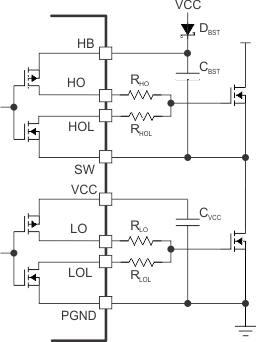 Figure 30. Drivers
