SNVSC09 March   2022 LM5143

PRODUCTION DATA  

  1. Features
  2. Applications
  3. Description
  4. Revision History
  5. Description (continued)
  6. Device Comparison Table
  7. Pin Configuration and Functions
  8. Specifications
    1. 8.1 Absolute Maximum Ratings
    2. 8.2 ESD Ratings
    3. 8.3 Recommended Operating Conditions
    4. 8.4 Thermal Information
    5. 8.5 Electrical Characteristics
    6. 8.6 Switching Characteristics
    7. 8.7 Typical Characteristics
  9. Detailed Description
    1. 9.1 Overview
    2. 9.2 Functional Block Diagram
    3. 9.3 Feature Description
      1. 9.3.1  Input Voltage Range (VIN)
      2. 9.3.2  High-Voltage Bias Supply Regulator (VCC, VCCX, VDDA)
      3. 9.3.3  Enable (EN1, EN2)
      4. 9.3.4  Power-Good Monitor (PG1, PG2)
      5. 9.3.5  Switching Frequency (RT)
      6. 9.3.6  Clock Synchronization (DEMB)
      7. 9.3.7  Synchronization Out (SYNCOUT)
      8. 9.3.8  Spread Spectrum Frequency Modulation (DITH)
      9. 9.3.9  Configurable Soft Start (SS1, SS2)
      10. 9.3.10 Output Voltage Setpoint (FB1, FB2)
      11. 9.3.11 Minimum Controllable On Time
      12. 9.3.12 Error Amplifier and PWM Comparator (FB1, FB2, COMP1, COMP2)
      13. 9.3.13 Slope Compensation
      14. 9.3.14 Inductor Current Sense (CS1, VOUT1, CS2, VOUT2)
        1. 9.3.14.1 Shunt Current Sensing
        2. 9.3.14.2 Inductor DCR Current Sensing
      15. 9.3.15 Hiccup Mode Current Limiting (RES)
      16. 9.3.16 High-Side and Low-Side Gate Drivers (HO1/2, LO1/2, HOL1/2, LOL1/2)
      17. 9.3.17 Output Configurations (MODE, FB2)
        1. 9.3.17.1 Independent Dual-Output Operation
        2. 9.3.17.2 Single-Output Interleaved Operation
        3. 9.3.17.3 Single-Output Multiphase Operation
    4. 9.4 Device Functional Modes
      1. 9.4.1 Standby Modes
      2. 9.4.2 Diode Emulation Mode
      3. 9.4.3 Thermal Shutdown
  10. 10Application and Implementation
    1. 10.1 Application Information
      1. 10.1.1 Power Train Components
        1. 10.1.1.1 Buck Inductor
        2. 10.1.1.2 Output Capacitors
        3. 10.1.1.3 Input Capacitors
        4. 10.1.1.4 Power MOSFETs
        5. 10.1.1.5 EMI Filter
      2. 10.1.2 Error Amplifier and Compensation
    2. 10.2 Typical Applications
      1. 10.2.1 Design 1 – 5-V and 3.3-V Dual-Output Buck Regulator for Computing Applications
        1. 10.2.1.1 Design Requirements
        2. 10.2.1.2 Detailed Design Procedure
          1. 10.2.1.2.1 Custom Design With WEBENCH® Tools
          2. 10.2.1.2.2 Custom Design With Excel Quickstart Tool
          3. 10.2.1.2.3 Inductor Calculation
          4. 10.2.1.2.4 Current-Sense Resistance
          5. 10.2.1.2.5 Output Capacitors
          6. 10.2.1.2.6 Input Capacitors
          7. 10.2.1.2.7 Compensation Components
        3. 10.2.1.3 Application Curves
      2. 10.2.2 Design 2 – Two-Phase, 15-A, 2.1-MHz Single-Output Buck Regulator for Server Applications
        1. 10.2.2.1 Design Requirements
        2. 10.2.2.2 Detailed Design Procedure
        3. 10.2.2.3 Application Curves
      3. 10.2.3 Design 3 – Two-Phase, 50-A, 300-kHz Single-Output Buck Regulator for ASIC Power Applications
        1. 10.2.3.1 Design Requirements
        2. 10.2.3.2 Detailed Design Procedure
        3. 10.2.3.3 Application Curves
  11. 11Power Supply Recommendations
  12. 12Layout
    1. 12.1 Layout Guidelines
      1. 12.1.1 Power Stage Layout
      2. 12.1.2 Gate-Drive Layout
      3. 12.1.3 PWM Controller Layout
      4. 12.1.4 Thermal Design and Layout
      5. 12.1.5 Ground Plane Design
    2. 12.2 Layout Example
  13. 13Device and Documentation Support
    1. 13.1 Device Support
      1. 13.1.1 Third-Party Products Disclaimer
      2. 13.1.2 Development Support
        1. 13.1.2.1 Custom Design With WEBENCH® Tools
    2. 13.2 Documentation Support
      1. 13.2.1 Related Documentation
        1. 13.2.1.1 PCB Layout Resources
        2. 13.2.1.2 Thermal Design Resources
    3. 13.3 Receiving Notification of Documentation Updates
    4. 13.4 Support Resources
    5. 13.5 Trademarks
    6. 13.6 Electrostatic Discharge Caution
    7. 13.7 Glossary
  14. 14Mechanical, Packaging, and Orderable Information

Package Options

Mechanical Data (Package|Pins)
Thermal pad, mechanical data (Package|Pins)
Orderable Information

Error Amplifier and Compensation

Figure 10-3 shows a Type-II compensator using a transconductance error amplifier (EA). The dominant pole of the EA open-loop gain is set by the EA output resistance, RO-EA, and effective bandwidth-limiting capacitance, CBW, as shown in Equation 28.

Equation 28. GUID-B6866D7B-3EA2-4253-8D85-6FB80BC81BEA-low.gif

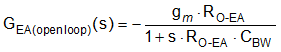
The EA high-frequency pole is neglected in Equation 28. The compensator transfer function from output voltage to COMP node, including the gain contribution from the (internal or external) feedback resistor network, is calculated in Equation 29.
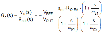
Equation 29. GUID-C156DE60-6CCE-4154-AD51-2B6C8E792F45-low.gif

where

  • VREF is the feedback voltage reference of 0.6 V.
  • gm is the EA gain transconductance of 1200 µS.
  • RO-EA is the error amplifier output impedance of 64 MΩ.
Equation 30. GUID-29DB74F9-C32C-4CC5-A569-493C39B52F6E-low.gif
Equation 31. GUID-3CB99734-6E57-4170-AFAC-FC24ED75EC0C-low.gif
Equation 32. GUID-2E7A4756-CFE1-4327-819B-DCFF41D483EB-low.gif

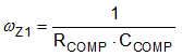
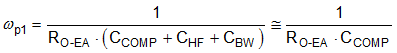
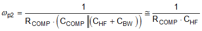
The EA compensation components create a pole close to the origin, a zero, and a high-frequency pole. Typically, RCOMP << RO-EA and CCOMP >> CBW and CHF, so the approximations are valid.

Figure 10-3 Error Amplifier and Compensation Network