SNVSBN8A December 2019 – April 2023 LM5163H-Q1
PRODUCTION DATA
- 1 Features
- 2 Applications
- 3 Description
- 4 Revision History
- 5 Pin Configuration and Functions
- 6 Specifications
-
7 Detailed Description
- 7.1 Overview
- 7.2 Functional Block Diagram
- 7.3
Feature Description
- 7.3.1 Control Architecture
- 7.3.2 Internal VCC Regulator and Bootstrap Capacitor
- 7.3.3 Regulation Comparator
- 7.3.4 Internal Soft Start
- 7.3.5 On-Time Generator
- 7.3.6 Current Limit
- 7.3.7 N-Channel Buck Switch and Driver
- 7.3.8 Synchronous Rectifier
- 7.3.9 Enable/Undervoltage Lockout (EN/UVLO)
- 7.3.10 Power Good (PGOOD)
- 7.3.11 Thermal Protection
- 7.4 Device Functional Modes
- 8 Application and Implementation
- 9 Device and Documentation Support
- 10Mechanical, Packaging, and Orderable Information
Package Options
Mechanical Data (Package|Pins)
- DDA|8
Thermal pad, mechanical data (Package|Pins)
- DDA|8
Orderable Information
8.2 Typical Application
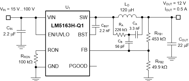
Figure 8-1 shows the schematic for a 12-V, 0.5-A COT converter.
 Figure 8-1 Typical Application VIN(nom) = 48 V, VOUT = 12 V, IOUT(max) = 0.5 A, FSW(nom) = 300 kHz
Note:
This and subsequent design examples are provided herein to showcase the LM5163H-Q1 converter in several different applications. Depending on the source impedance of the input supply bus, an electrolytic capacitor may be required at the input to ensure stability, particularly at low input voltage and high output current operating conditions. See the Section 8.3 section for more details.