SNVSAI1D June 2017 – August 2021 LM5176
PRODUCTION DATA
- 1 Features
- 2 Applications
- 3 Description
- 4 Revision History
- 5 Pin Configuration and Functions
- 6 Specifications
-
7 Detailed Description
- 7.1 Overview
- 7.2 Functional Block Diagram
- 7.3
Feature Description
- 7.3.1 Fixed Frequency Valley/Peak Current Mode Control with Slope Compensation
- 7.3.2 VCC Regulator and Optional BIAS Input
- 7.3.3 Enable/UVLO
- 7.3.4 Soft Start
- 7.3.5 Overcurrent Protection
- 7.3.6 Average Input/Output Current Limiting
- 7.3.7 Operation Above 40-V Input
- 7.3.8 CCM Operation
- 7.3.9 Frequency and Synchronization (RT/SYNC)
- 7.3.10 Frequency Dithering
- 7.3.11 Output Overvoltage Protection (OVP)
- 7.3.12 Power Good (PGOOD)
- 7.3.13 Gm Error Amplifier
- 7.3.14 Integrated Gate Drivers
- 7.3.15 Thermal Shutdown
- 7.4 Device Functional Modes
-
8 Application and Implementation
- 8.1 Application Information
- 8.2
Typical Application
- 8.2.1 Design Requirements
- 8.2.2
Detailed Design Procedure
- 8.2.2.1 Custom Design with WEBENCH Tools
- 8.2.2.2 Frequency
- 8.2.2.3 VOUT
- 8.2.2.4 Inductor Selection
- 8.2.2.5 Output Capacitor
- 8.2.2.6 Input Capacitor
- 8.2.2.7 Sense Resistor (RSENSE)
- 8.2.2.8 Slope Compensation
- 8.2.2.9 UVLO
- 8.2.2.10 Soft-Start Capacitor
- 8.2.2.11 Dither Capacitor
- 8.2.2.12 MOSFETs QH1 and QL1
- 8.2.2.13 MOSFETs QH2 and QL2
- 8.2.2.14 Frequency Compensation
- 8.2.3 Application Curves
- 9 Power Supply Recommendations
- 10Layout
- 11Device and Documentation Support
- 12Mechanical, Packaging, and Orderable Information
Package Options
Mechanical Data (Package|Pins)
Thermal pad, mechanical data (Package|Pins)
Orderable Information
8.2.2.9 UVLO
The UVLO resistor divider must be designed for turnon below 6 V. Selecting RUV2 = 249 kΩ gives a UVLO hysteresis of 0.8 V based on Equation 2. The lower UVLO resistor is the selected using Equation 27:
Equation 27. 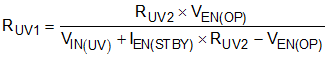
A standard value of 59.0 kΩ is selected for RUV1.
When programming the UVLO threshold for lower input voltage operation, it is important to choose MOSFETs with gate (Miller) plateau voltage lower than the minimum VIN.