SNVSAI1D June 2017 – August 2021 LM5176
PRODUCTION DATA
- 1 Features
- 2 Applications
- 3 Description
- 4 Revision History
- 5 Pin Configuration and Functions
- 6 Specifications
-
7 Detailed Description
- 7.1 Overview
- 7.2 Functional Block Diagram
- 7.3
Feature Description
- 7.3.1 Fixed Frequency Valley/Peak Current Mode Control with Slope Compensation
- 7.3.2 VCC Regulator and Optional BIAS Input
- 7.3.3 Enable/UVLO
- 7.3.4 Soft Start
- 7.3.5 Overcurrent Protection
- 7.3.6 Average Input/Output Current Limiting
- 7.3.7 Operation Above 40-V Input
- 7.3.8 CCM Operation
- 7.3.9 Frequency and Synchronization (RT/SYNC)
- 7.3.10 Frequency Dithering
- 7.3.11 Output Overvoltage Protection (OVP)
- 7.3.12 Power Good (PGOOD)
- 7.3.13 Gm Error Amplifier
- 7.3.14 Integrated Gate Drivers
- 7.3.15 Thermal Shutdown
- 7.4 Device Functional Modes
-
8 Application and Implementation
- 8.1 Application Information
- 8.2
Typical Application
- 8.2.1 Design Requirements
- 8.2.2
Detailed Design Procedure
- 8.2.2.1 Custom Design with WEBENCH Tools
- 8.2.2.2 Frequency
- 8.2.2.3 VOUT
- 8.2.2.4 Inductor Selection
- 8.2.2.5 Output Capacitor
- 8.2.2.6 Input Capacitor
- 8.2.2.7 Sense Resistor (RSENSE)
- 8.2.2.8 Slope Compensation
- 8.2.2.9 UVLO
- 8.2.2.10 Soft-Start Capacitor
- 8.2.2.11 Dither Capacitor
- 8.2.2.12 MOSFETs QH1 and QL1
- 8.2.2.13 MOSFETs QH2 and QL2
- 8.2.2.14 Frequency Compensation
- 8.2.3 Application Curves
- 9 Power Supply Recommendations
- 10Layout
- 11Device and Documentation Support
- 12Mechanical, Packaging, and Orderable Information
Package Options
Mechanical Data (Package|Pins)
Thermal pad, mechanical data (Package|Pins)
Orderable Information
7.3.3 Enable/UVLO
The LM5176 has a dual function enable and undervoltage lockout (UVLO) circuit. The EN/UVLO pin has three distinct voltage ranges: shutdown, standby, and operating (see Section 7.4.1). When the EN/UVLO pin is below the standby threshold, VEN(STBY), the converter is held in a low power shutdown mode. When EN/UVLO voltage is greater than the standby threshold, VEN(STBY), but less than the operating threshold, VEN(OP), the internal bias rails and the VCC regulator are enabled but the soft-start (SS) pin is held low and the PWM controller is disabled. A pullup current IEN(STBY) is sourced out of the EN/UVLO pin in standby mode to provide hysteresis between the shutdown mode and the standby mode. When EN/UVLO is greater than the operating threshold, VEN(OP), and VCC is above the undervoltage threshold, VUV(VCC), the controller starts operation. A hysteresis current ΔIHYS(OP) is sourced out of the EN/UVLO pin when the EN/UVLO input exceeds the operating threshold to provide hysteresis that prevents on/off chattering in the presence of noise with a slowly changing input voltage.
The VIN UVLO threshold is typically set by a resistor divider from VIN to AGND (Figure 7-2). The turnon threshold VIN(UV) is calculated using Equation 1 where RUV2 is the upper resistor and RUV1 is the lower resistor in the EN/UVLO resistor divider:
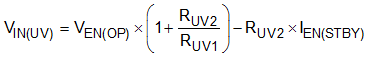
The hysteresis between the UVLO turnon threshold and turnoff threshold is set by the upper resistor in the EN/UVLO resistor divider and is given by:
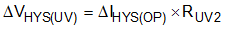
 Figure 7-2 UVLO Threshold Programming