SNVSBU4D june 2022 – august 2023 LM5177
PRODUCTION DATA
- 1
- 1 Features
- 2 Applications
- 3 Description
- 4 Revision History
- 5 Pin Configuration and Functions
- 6 Specifications
- 7 Parameter Measurement Information
-
8 Detailed Description
- 8.1 Overview
- 8.2 Functional Block Diagram
- 8.3
Feature Description
- 8.3.1 Power-On Reset (POR System)
- 8.3.2 Buck-Boost Control Scheme
- 8.3.3 Power Save Mode
- 8.3.4 Supply Voltage Selection – VMAX Switch
- 8.3.5 Enable and Undervoltage Lockout
- 8.3.6 Oscillator Frequency Selection
- 8.3.7 Frequency Synchronization
- 8.3.8 Voltage Regulation Loop
- 8.3.9 Output Voltage Tracking
- 8.3.10 Slope Compensation
- 8.3.11 Configurable Soft Start
- 8.3.12 Peak Current Sensor
- 8.3.13 Current Monitoring and Current Limit Control Loop
- 8.3.14 Short Circuit - Hiccup Protection
- 8.3.15 nFLT Pin and Protections
- 8.3.16 Device Configuration Pin
- 8.3.17 Dual Random Spread Spectrum – DRSS
- 8.3.18 Gate Driver
- 8.4 Device Functional Modes
-
9 Application and Implementation
- 9.1 Application Information
- 9.2
Typical Application
- 9.2.1 Design Requirements
- 9.2.2
Detailed Design Procedure
- 9.2.2.1 Custom Design with WEBENCH Tools
- 9.2.2.2 Frequency
- 9.2.2.3 Feedback Divider
- 9.2.2.4 Inductor and Current Sense Resistor Selection
- 9.2.2.5 Slope Compensation
- 9.2.2.6 Output Capacitor
- 9.2.2.7 Input Capacitor
- 9.2.2.8 UVLO Divider
- 9.2.2.9 Soft-Start Capacitor
- 9.2.2.10 MOSFETs QH1 and QL1
- 9.2.2.11 MOSFETs QH2 and QL2
- 9.2.2.12 Frequency Compensation
- 9.2.2.13 External Component Selection
- 9.2.3 Application Curves
- 9.3 System Examples
- 10Power Supply Recommendations
- 11Layout
- 12Device and Documentation Support
- 13Mechanical, Packaging, and Orderable Information
Package Options
Mechanical Data (Package|Pins)
- DCP|38
Thermal pad, mechanical data (Package|Pins)
- DCP|38
Orderable Information
8.3.4 Supply Voltage Selection – VMAX Switch
There are two pins to supply the LM5177 internal voltage regulators. Due to the internal supply voltage selection circuit, the device can reduce the power dissipation by ensuring a seamless operation at low input or output voltages as well as in transient operating conditions like an output short. The VMAX switch selects the pin with the lower voltage from the VIN or BIAS pin once the voltage on both is above the switch-over threshold (VT(VCC, SUP)). If one pin voltage is lower than the threshold, the other supply pin is selected. And if both pins are lower than the switch-over threshold, the higher voltage of VIN or BIAS is selected as supply. The following are common configurations for the supply pins:
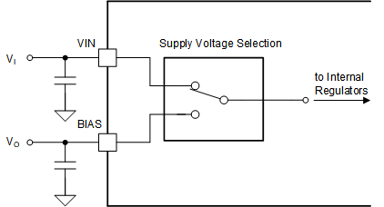
- The VIN pin is connected to the supply voltage. The BIAS pin is connected to VO. During start-up, that is as long as the output voltage is not higher than the supply switch-over threshold, the VIN supplies the internal regulators. Once VO is high enough, the supply current comes from the BIAS pin.
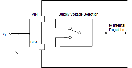
- Both the VIN pin and the BIAS pin are connected together to the input supply voltage. This configuration is often used in applications where the input supply voltage is usually lower or equal than the output voltage. As the BIAS pin is connected to the input voltage, the device has the full current capability of the internal regulators at low input voltages for start-up.
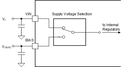
- The VIN is connected to the input supply voltage and the BIAS pin is connected to an auxiliary supply (for example, an existing 12-V DC/DC converter). This configuration is commonly used at high voltage applications on the input and output voltages where the power dissipation over the integrated linear regulators must be further minimized.

Figure 8-6 VMAX Supply Scenario 1
 Figure 8-7 VMAX Supply Scenario 2
Figure 8-8 VMAX Supply Scenario 3