SNVSBM6A April 2020 – January 2021 LM5181
PRODUCTION DATA
- 1 Features
- 2 Applications
- 3 Description
- 4 Revision History
- 5 Description (continued)
- 6 Pin Configuration and Functions
- 7 Specifications
-
8 Detailed Description
- 8.1 Overview
- 8.2 Functional Block Diagram
- 8.3
Feature Description
- 8.3.1 Integrated Power MOSFET
- 8.3.2 PSR Flyback Modes of Operation
- 8.3.3 Setting the Output Voltage
- 8.3.4 Control Loop Error Amplifier
- 8.3.5 Precision Enable
- 8.3.6 Configurable Soft Start
- 8.3.7 External Bias Supply
- 8.3.8 Minimum On-Time and Off-Time
- 8.3.9 Overcurrent Protection
- 8.3.10 Thermal Shutdown
- 8.4 Device Functional Modes
-
9 Application and Implementation
- 9.1 Application Information
- 9.2
Typical Applications
- 9.2.1
Design 1: Wide VIN, Low IQ PSR Flyback Converter Rated at 5 V, 0.5 A
- 9.2.1.1 Design Requirements
- 9.2.1.2
Detailed Design Procedure
- 9.2.1.2.1 Custom Design With WEBENCH® Tools
- 9.2.1.2.2 Custom Design With Excel Quickstart Tool
- 9.2.1.2.3 Flyback Transformer – T1
- 9.2.1.2.4 Flyback Diode – DFLY
- 9.2.1.2.5 Zener Clamp Circuit – DF, DCLAMP
- 9.2.1.2.6 Output Capacitor – COUT
- 9.2.1.2.7 Input Capacitor – CIN
- 9.2.1.2.8 Feedback Resistor – RFB
- 9.2.1.2.9 Thermal Compensation Resistor – RTC
- 9.2.1.2.10 UVLO Resistors – RUV1, RUV2
- 9.2.1.2.11 Soft-Start Capacitor – CSS
- 9.2.2 Application Curves
- 9.2.1
Design 1: Wide VIN, Low IQ PSR Flyback Converter Rated at 5 V, 0.5 A
- 10Power Supply Recommendations
- 11Layout
- 12Device and Documentation Support
- 13Mechanical, Packaging, and Orderable Information
Package Options
Mechanical Data (Package|Pins)
- NGU|8
Thermal pad, mechanical data (Package|Pins)
Orderable Information
8.3.5 Precision Enable
The precision EN/UVLO input supports adjustable input undervoltage lockout (UVLO) with hysteresis for application specific power-up and power-down requirements. EN/UVLO connects to a comparator with a 1.5-V reference voltage and 50-mV hysteresis. An external logic signal can be used to drive the EN/UVLO input to toggle the output on and off for system sequencing or protection. The simplest way to enable the LM5181 is to connect EN/UVLO directly to VIN. This allows the LM5181 to start up when VIN is within its valid operating range. However, many applications benefit from using a resistor divider RUV1 and RUV2 as shown in Figure 8-3 to establish a precision UVLO level.
 Figure 8-3 Programmable Input Voltage UVLO With Hysteresis
Use Equation 10 and Equation 11 to calculate the input UVLO voltages turnon and turnoff voltages, respectively.
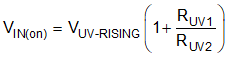
where
- VUV-RISING and VUV-FALLING are the UVLO comparator thresholds
- IUV-HYST is the hysteresis current
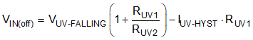
where
- VUV-RISING and VUV-FALLING are the UVLO comparator thresholds
- IUV-HYST is the hysteresis current
The LM5181 also provides a low-IQ shutdown mode when the EN/UVLO voltage is pulled below a base-emitter voltage drop (approximately 0.6 V at room temperature). If the EN/UVLO voltage is below this hard shutdown threshold, the internal LDO regulator powers off, and the internal bias-supply rail collapses, shutting down the bias currents of the LM5181. The LM5181 operates in standby mode when the EN/UVLO voltage is between the hard shutdown and precision-enable thresholds.