SNAS660D June 2015 – May 2021 LM53600-Q1 , LM53601-Q1
PRODUCTION DATA
- 1 Features
- 2 Applications
- 3 Description
- 4 Revision History
- 5 Device Comparison
- 6 Pin Configuration and Functions
- 7 Specifications
- 8 Detailed Description
- 9 Applications and Implementation
- 10Power Supply Recommendations
- 11Layout
- 12Device and Documentation Support
- 13Mechanical, Packaging, and Orderable Information
Package Options
Mechanical Data (Package|Pins)
- DSX|10
Thermal pad, mechanical data (Package|Pins)
- DSX|10
Orderable Information
8.3.7 Auto Mode Operation and IQ_VIN
If SYNC/MODE is held low for a period greater than a few microseconds, the LM53600-Q1 and LM53601-Q1 devices will enable automatic power saving light load operation and diode emulation. In this mode, if peak current needed to regulate output voltage drops below a selected value, the clock of the LM53600-Q1 or LM53601-Q1 device slows to maintain regulation. The gain of this clock slowing circuit is low to maintain stability. Output voltage with no load is approximately 1% higher than with a load high enough to allow full frequency operation.
IQ_VIN is the current consumed by a converter utilizing a LM53600-Q1 or LM53601-Q1 device while regulating without a load. While operating without a load, the LM53600-Q1 or LM53601-Q1 is only powering itself. The LM53600-Q1 and LM53601-Q1 device draws power from two sources, its VIN pin, IQ, and either its FB pin for fixed versions or BIAS pin for adjustable versions, IB. Since BIAS or FB is connected to the circuit’s output, the power consumed is converted from input power with an effective efficiency, ηeff, of ~80%. Here, effective efficiency is the added input power needed when lightly loading the converter of the LM53600-Q1 and LM53601-Q1 devices is divided by the corresponding additional load. This allows unloaded current to be calculated as follows:
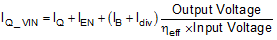
where
- IQ_VIN is the current consumed by the Buck converter utilizing the LM53600-Q1 or LM53601-Q1 while unloaded.
- IQ is the current drawn by the LM53600-Q1 or LM53601-Q1 from its VIN terminal. See IQ in section 7.6.
- IEN is current drawn by the LM53600-Q1 or LM53601-Q1 from its EN terminal. Include this current if EN is connected to VIN. See IEN in section 7.6. Note that this current drops to a very low value if connected to a voltage less than 5 V.
- IB is bias/feedback current drawn by the LM53600-Q1 or LM53601-Q1 while the Buck converter utilizing it is unloaded. See IB in section 7.6.
- Idiv is the current drawn by the feedback voltage divider used to set output voltage for adjustable devices. This current is zero for fixed output voltage devices.
- ηeff is the light load efficiency of the Buck converter with IQ_VIN removed from the Buck converter’s input current. 0.8 is a conservative value that can be used under normal operating conditions
Note that the EN pin consumes a few microamperes when tied to high; see IEN. Add IEN to IQ as shown in the above equation if EN is tied to VIN. If EN is tied to a voltage less than 5 V, virtually no current is consumed allowing EN to be used as a UVL once a voltage divider is added.