SNAS548D February 2000 – January 2015 LM555
PRODUCTION DATA.
- 1 Features
- 2 Applications
- 3 Description
- 4 Revision History
- 5 Pin Configuration and Functions
- 6 Specifications
- 7 Detailed Description
- 8 Application and Implementation
- 9 Power Supply Recommendations
- 10Layout
- 11Device and Documentation Support
- 12Mechanical, Packaging, and Orderable Information
Package Options
Mechanical Data (Package|Pins)
Thermal pad, mechanical data (Package|Pins)
Orderable Information
7 Detailed Description
7.1 Overview
The LM555 is a highly stable device for generating accurate time delays or oscillation. Additional terminals are provided for triggering or resetting if desired. In the time delay mode of operation, the time is precisely controlled by one external resistor and capacitor. For astable operation as an oscillator, the free running frequency and duty cycle are accurately controlled with two external resistors and one capacitor. The circuit may be triggered and reset on falling waveforms, and the output circuit can source or sink up to 200mA or driver TTL circuits. The LM555 are available in 8-pin PDIP, SOIC, and VSSOP packages and is a direct replacement for SE555/NE555.
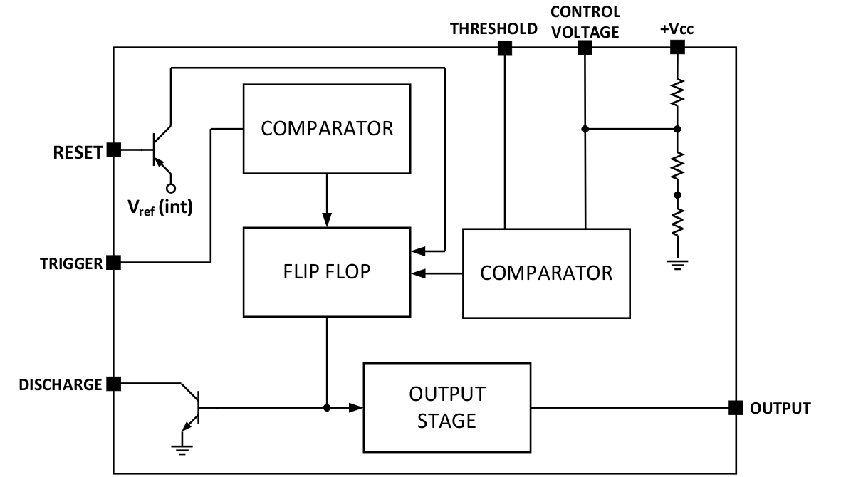
7.2 Functional Block Diagram
7.3 Feature Description
7.3.1 Direct Replacement for SE555/NE555
The LM555 timer is a direct replacement for SE555 and NE555. It is pin-to-pin compatible so that no schematic or layout changes are necessary. The LM555 come in an 8-pin PDIP, SOIC, and VSSOP package.
7.3.2 Timing From Microseconds Through Hours
The LM555 has the ability to have timing parameters from the microseconds range to hours. The time delay of the system can be determined by the time constant of the R and C value used for either the monostable or astable configuration. A nomograph is available for easy determination of R and C values for various time delays.
7.3.3 Operates in Both Astable and Monostable Mode
The LM555 can operate in both astable and monostable mode depending on the application requirements.
- Monostable mode: The LM555 timer acts as a “one-shot” pulse generator. The pulse beings when the LM555 timer receives a signal at the trigger input that falls below a 1/3 of the voltage supply. The width of the output pulse is determined by the time constant of an RC network. The output pulse ends when the voltage on the capacitor equals 2/3 of the supply voltage. The output pulse width can be extended or shortened depending on the application by adjusting the R and C values.
- Astable (free-running) mode: The LM555 timer can operate as an oscillator and puts out a continuous stream of rectangular pulses having a specified frequency. The frequency of the pulse stream depends on the values of RA, RB, and C.
7.4 Device Functional Modes
7.4.1 Monostable Operation
In this mode of operation, the timer functions as a one-shot (Figure 11). The external capacitor is initially held discharged by a transistor inside the timer. Upon application of a negative trigger pulse of less than 1/3 VCC to pin 2, the flip-flop is set which both releases the short circuit across the capacitor and drives the output high.
 Figure 11. Monostable
The voltage across the capacitor then increases exponentially for a period of t = 1.1 RA C, at the end of which time the voltage equals 2/3 VCC. The comparator then resets the flip-flop which in turn discharges the capacitor and drives the output to its low state. Figure 12 shows the waveforms generated in this mode of operation. Since the charge and the threshold level of the comparator are both directly proportional to supply voltage, the timing interval is independent of supply.
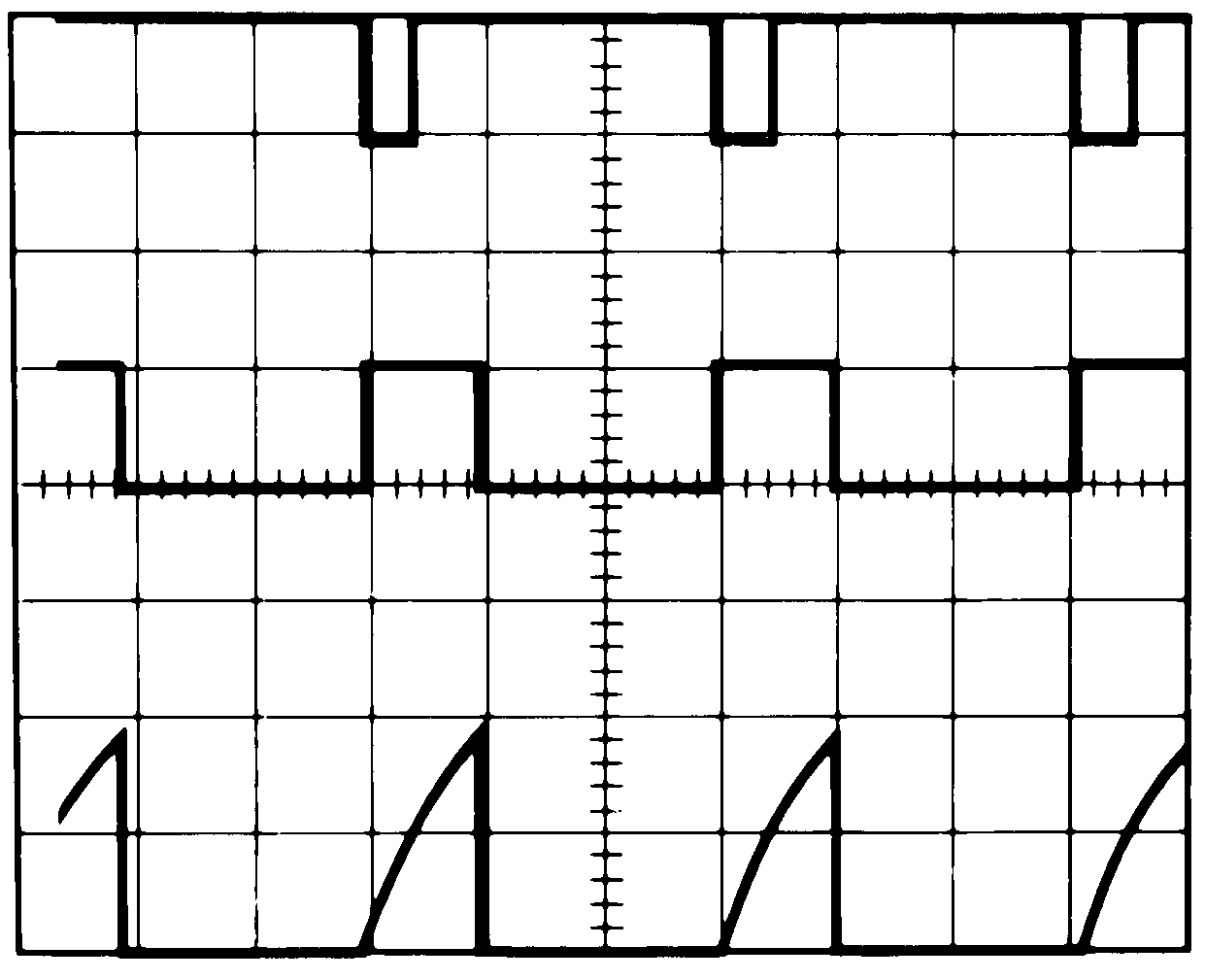
TIME = 0.1 ms/DIV. Middle Trace: Output 5V/Div.
RA = 9.1 kΩ Bottom Trace: Capacitor Voltage 2V/Div.
C = 0.01 μF
During the timing cycle when the output is high, the further application of a trigger pulse will not effect the circuit so long as the trigger input is returned high at least 10 μs before the end of the timing interval. However the circuit can be reset during this time by the application of a negative pulse to the reset terminal (pin 4). The output will then remain in the low state until a trigger pulse is again applied.
When the reset function is not in use, TI recommends connecting the Reset pin to VCC to avoid any possibility of false triggering.
Figure 13 is a nomograph for easy determination of R, C values for various time delays.
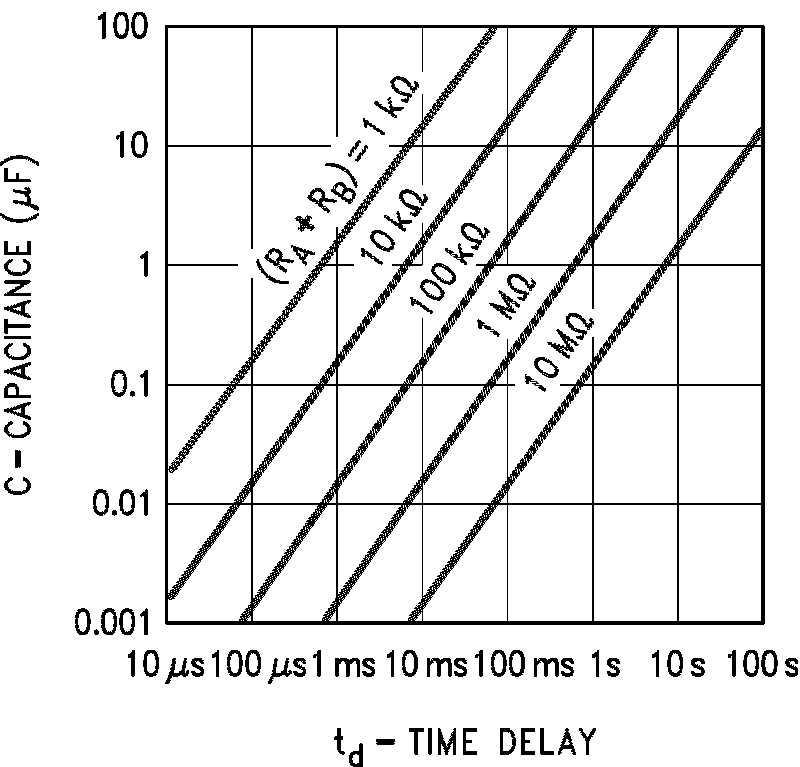 Figure 13. Time Delay
7.4.2 Astable Operation
If the circuit is connected as shown in Figure 14 (pins 2 and 6 connected) it will trigger itself and free run as a multivibrator. The external capacitor charges through RA + RB and discharges through RB. Thus the duty cycle may be precisely set by the ratio of these two resistors.
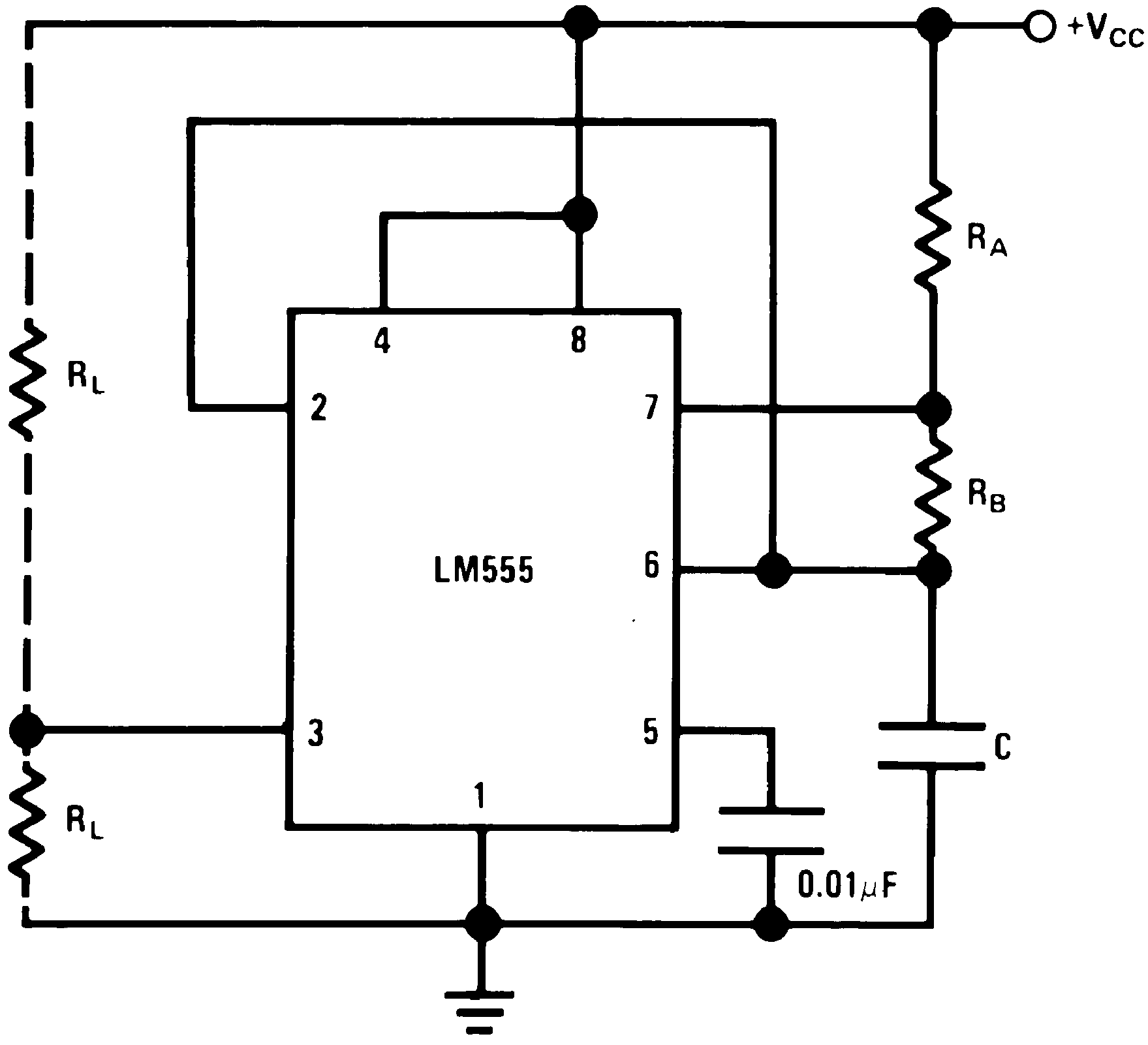 Figure 14. Astable
In this mode of operation, the capacitor charges and discharges between 1/3 VCC and 2/3 VCC. As in the triggered mode, the charge and discharge times, and therefore the frequency are independent of the supply voltage.
Figure 15 shows the waveforms generated in this mode of operation.
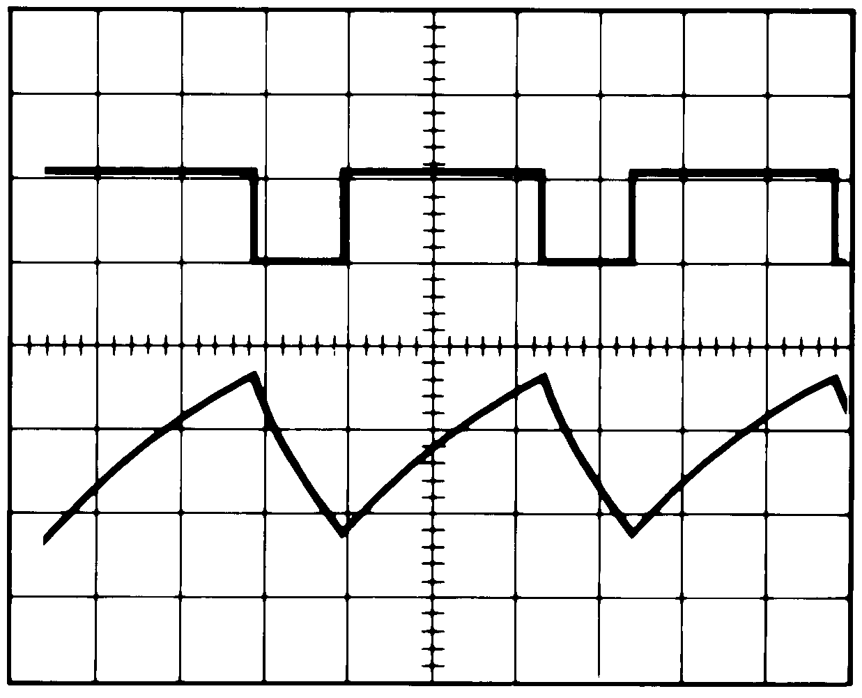
TIME = 20μs/DIV. Bottom Trace: Capacitor Voltage 1V/Div.
RA = 3.9 kΩ
RB = 3 kΩ
C = 0.01 μF
The charge time (output high) is given by:
And the discharge time (output low) by:
Thus the total period is:
The frequency of oscillation is:
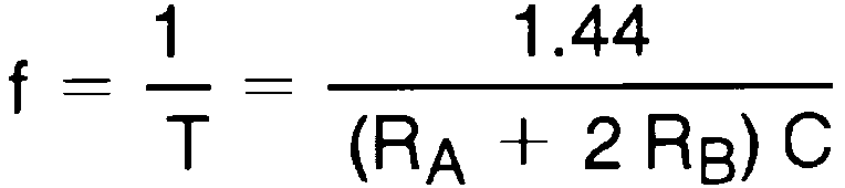
Figure 16 may be used for quick determination of these RC values.
The duty cycle is:
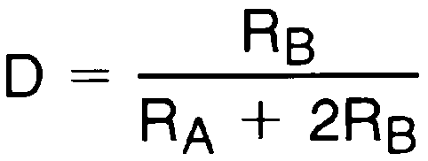
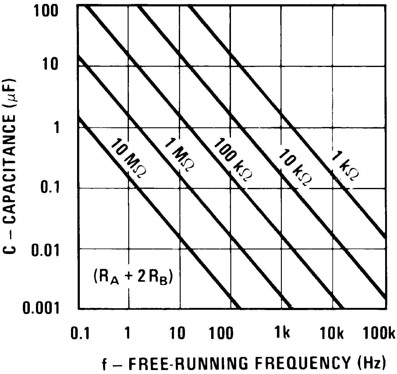 Figure 16. Free Running Frequency