SNAS548D February 2000 – January 2015 LM555
PRODUCTION DATA.
- 1 Features
- 2 Applications
- 3 Description
- 4 Revision History
- 5 Pin Configuration and Functions
- 6 Specifications
- 7 Detailed Description
- 8 Application and Implementation
- 9 Power Supply Recommendations
- 10Layout
- 11Device and Documentation Support
- 12Mechanical, Packaging, and Orderable Information
Package Options
Mechanical Data (Package|Pins)
Thermal pad, mechanical data (Package|Pins)
Orderable Information
8 Application and Implementation
NOTE
Information in the following applications sections is not part of the TI component specification, and TI does not warrant its accuracy or completeness. TI’s customers are responsible for determining suitability of components for their purposes. Customers should validate and test their design implementation to confirm system functionality.
8.1 Application Information
The LM555 timer can be used a various configurations, but the most commonly used configuration is in monostable mode. A typical application for the LM555 timer in monostable mode is to turn on an LED for a specific time duration. A pushbutton is used as the trigger to output a high pulse when trigger pin is pulsed low. This simple application can be modified to fit any application requirement.
8.2 Typical Application
Figure 17 shows the schematic of the LM555 that flashes an LED in monostable mode.
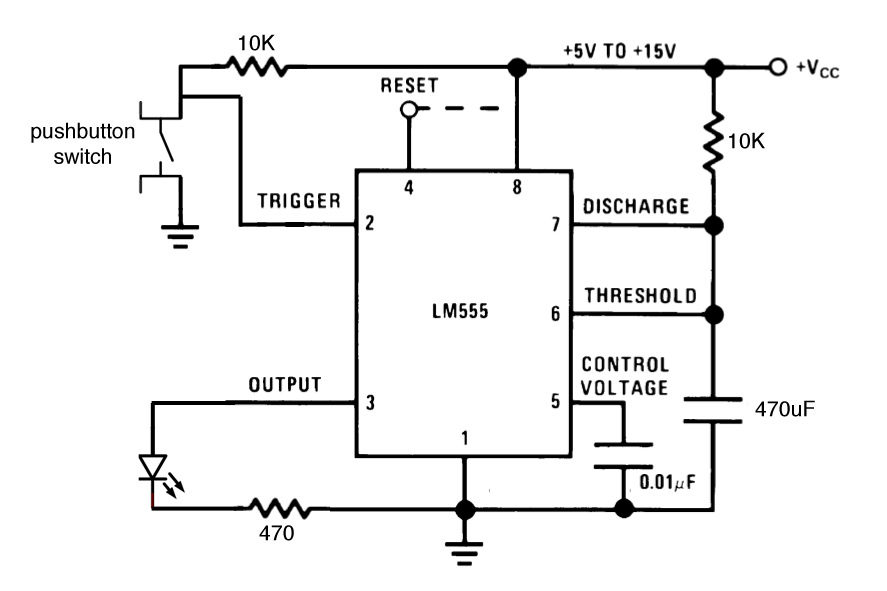 Figure 17. Schematic of Monostable Mode to Flash an LED
8.2.1 Design Requirements
The main design requirement for this application requires calculating the duration of time for which the output stays high. The duration of time is dependent on the R and C values (as shown in Figure 17) and can be calculated by:
8.2.2 Detailed Design Procedure
To allow the LED to flash on for a noticeable amount of time, a 5 second time delay was chosen for this application. By using Equation 6, RC equals 4.545. If R is selected as 100 kΩ, C = 45.4 µF. The values of R = 100 kΩ and C = 47 µF was selected based on standard values of resistors and capacitors. A momentary push button switch connected to ground is connected to the trigger input with a 10-K current limiting resistor pullup to the supply voltage. When the push button is pressed, the trigger pin goes to GND. An LED is connected to the output pin with a current limiting resistor in series from the output of the LM555 to GND. The reset pin is not used and was connected to the supply voltage.
8.2.2.1 Frequency Divider
The monostable circuit of Figure 11 can be used as a frequency divider by adjusting the length of the timing cycle. Figure 18 shows the waveforms generated in a divide by three circuit.
TIME = 20 μs/DIV. Middle Trace: Output 2V/Div.
RA = 9.1 kΩ Bottom Trace: Capa citor 2V/Div.
C = 0.01 μF
8.2.2.2 Additional Information
Lower comparator storage time can be as long as 10 μs when pin 2 is driven fully to ground for triggering. This limits the monostable pulse width to 10 μs minimum.
Delay time reset to output is 0.47 μs typical. Minimum reset pulse width must be 0.3 μs, typical.
Pin 7 current switches within 30 ns of the output (pin 3) voltage.
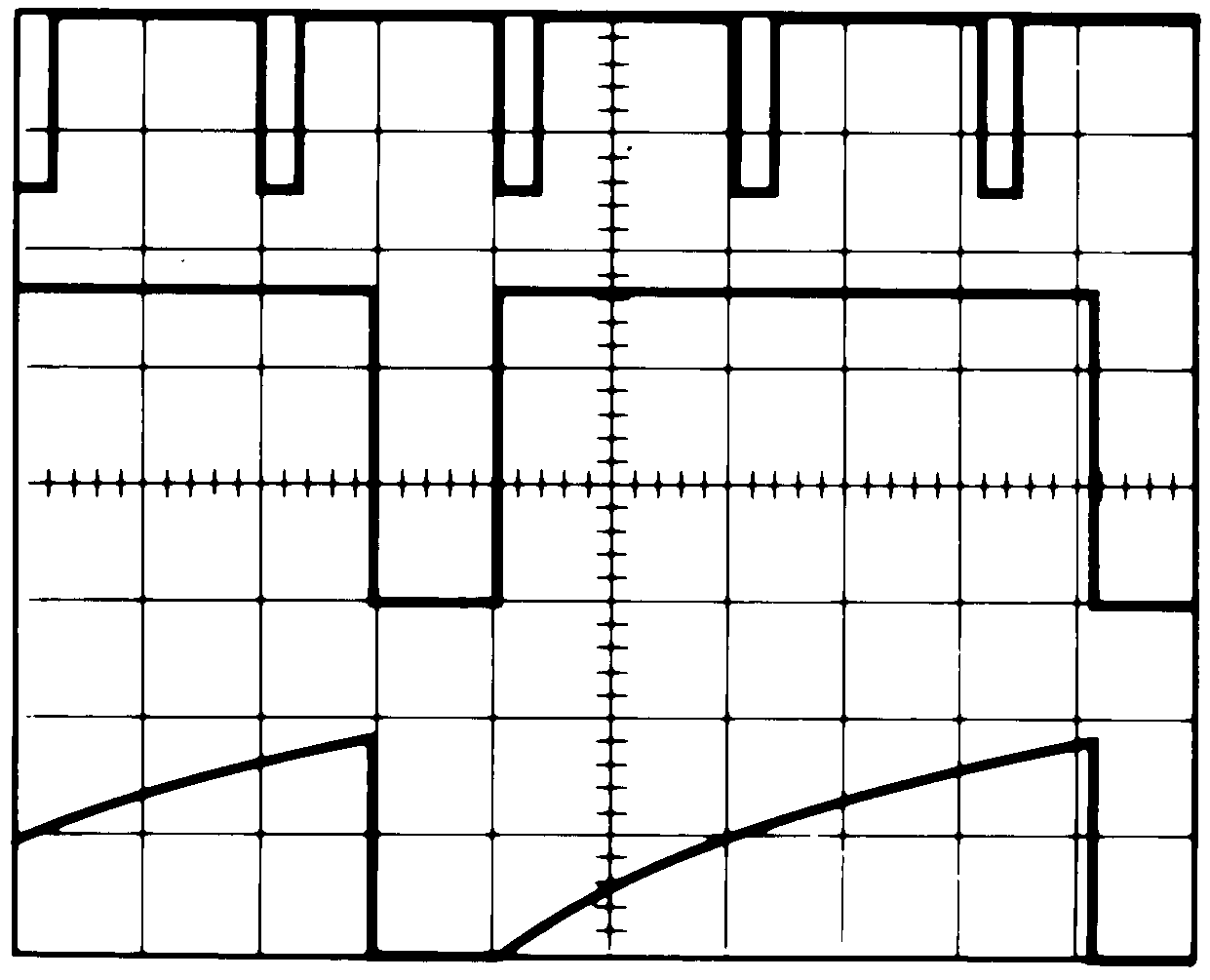
8.2.3 Application Curves
The data shown below was collected with the circuit used in the typical applications section. The LM555 was configured in the monostable mode with a time delay of 5.17 s. The waveforms correspond to:
- Top Waveform (Yellow) – Capacitor voltage
- Middle Waveform (Green) – Trigger
- Bottom Waveform (Purple) – Output
As the trigger pin pulses low, the capacitor voltage starts charging and the output goes high. The output goes low as soon as the capacitor voltage reaches 2/3 of the supply voltage, which is the time delay set by the R and C value. For this example, the time delay is 5.17 s.
 Figure 19. Trigger, Capacitor Voltage, and Output Waveforms in Monostable Mode