SNVSBN5A February 2020 – June 2020 LM60430 , LM60440
PRODUCTION DATA.
- 1 Features
- 2 Applications
- 3 Description
- 4 Revision History
- 5 Device Comparison Table
- 6 Pin Configuration and Functions
- 7 Specifications
- 8 Detailed Description
-
9 Application and Implementation
- 9.1 Application Information
- 9.2
Typical Application
- 9.2.1 Design Requirements
- 9.2.2
Detailed Design Procedure
- 9.2.2.1 Custom Design With WEBENCH® Tools
- 9.2.2.2 Choosing the Switching Frequency
- 9.2.2.3 Setting the Output Voltage
- 9.2.2.4 Inductor Selection
- 9.2.2.5 Output Capacitor Selection
- 9.2.2.6 Input Capacitor Selection
- 9.2.2.7 CBOOT
- 9.2.2.8 VCC
- 9.2.2.9 CFF Selection
- 9.2.2.10 External UVLO
- 9.2.2.11 Maximum Ambient Temperature
- 9.2.3 Application Curves
- 9.3 EMI
- 9.4 What to Do and What Not to Do
- 10Power Supply Recommendations
- 11Layout
- 12Device and Documentation Support
- 13Mechanical, Packaging, and Orderable Information
Package Options
Mechanical Data (Package|Pins)
- RPK|13
Thermal pad, mechanical data (Package|Pins)
Orderable Information
9.2.3 Application Curves
Unless otherwise specified the following conditions apply: VIN = 12 V, TA = 25°C. The circuit is shown in Figure 17, with the appropriate BOM from Table 4.
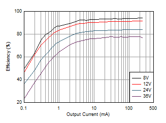
| VOUT = 5 V | 400 kHz | |
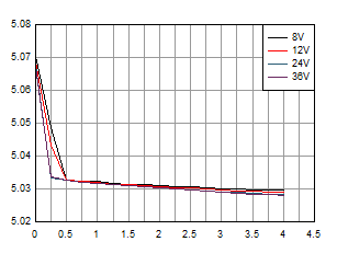
| VOUT = 5 V |
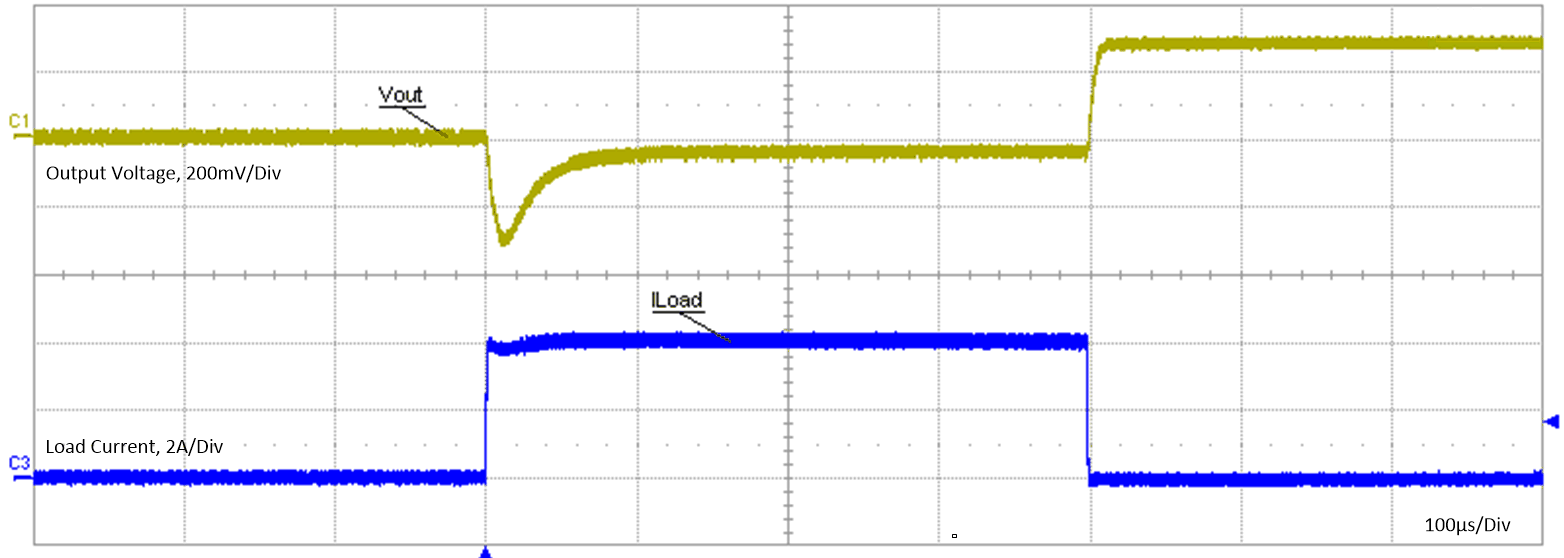
| VIN = 12 V | VOUT = 5 V | |
| IOUT = 0 A to 4 A | tf = tr = 4 µs | |
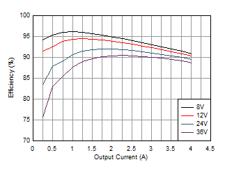
| VOUT = 5 V | 400 kHz | |
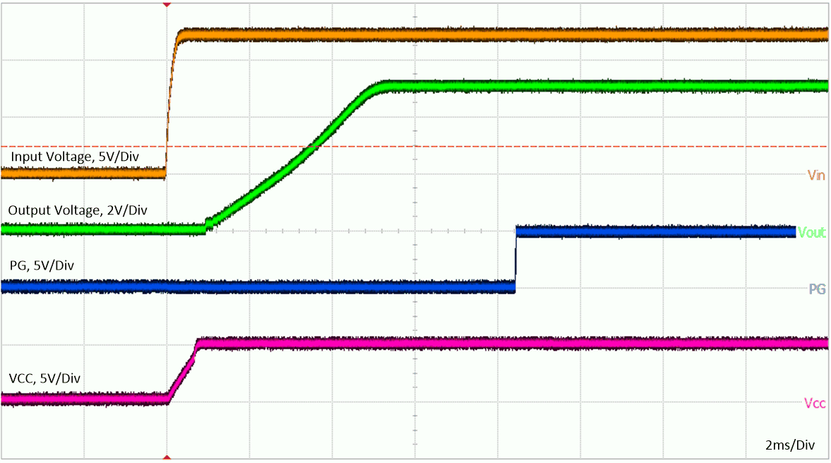
| VIN = 13.5 V | VOUT = 5 V | IOUT = 4 A | |
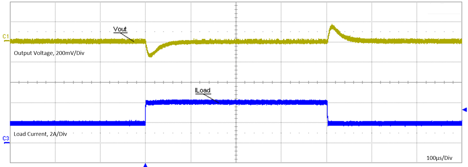
| VIN = 12 V | VOUT = 5 V | |
| tf = tr = 2 µs | IOUT = 2 A to 4 A | |
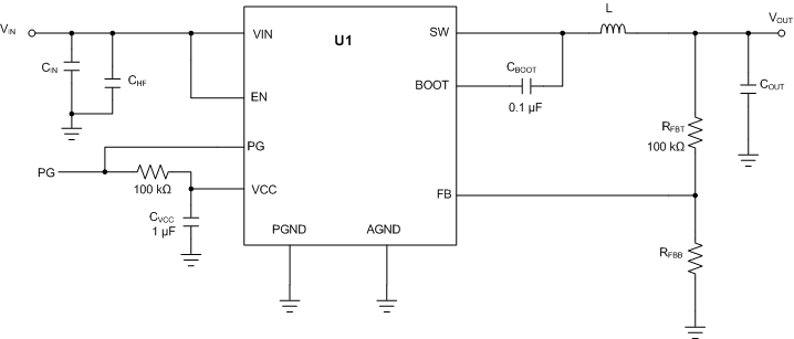 Figure 17. Circuit for Application Curves
 Table 4. BOM for Typical Application Curves
| VOUT | FREQUENCY | RFBB | COUT | CIN + CHF | L | U1 |
|---|---|---|---|---|---|---|
| 5 V | 400 kHz | 24.9 k | 2 x 47 µF + 22µF | 4.7 µF + 2 × 220 nF | 6.8 µH, 20.8 mΩ | LM60440ARPKPR |