SNOS745D May 1998 – November 2023 LM6171
PRODUCTION DATA
- 1
- 1 Features
- 2 Applications
- 3 Description
- 4 Pin Configuration and Functions
- 5 Specifications
- 6 Detailed Description
- 7 Application and Implementation
- 8 Device and Documentation Support
- 9 Revision History
- 10Mechanical, Packaging, and Orderable Information
Package Options
Refer to the PDF data sheet for device specific package drawings
Mechanical Data (Package|Pins)
- D|8
- P|8
Thermal pad, mechanical data (Package|Pins)
Orderable Information
3 Description
The LM6171 is a high-speed, unity-gain-stable voltage-feedback amplifier. The LM6171 offers a high slew rate of 3600 V/μs and a unity-gain bandwidth of 100 MHz while consuming only 2.5 mA of supply current. The LM6171 has very impressive ac and dc performance that is a great benefit for high-speed signal processing and video applications.
The ±15‑V power supplies allow for large signal swings and give greater dynamic range and signal-to-noise ratio (SNR). The LM6171 has a high output current drive, low spurious-free dynamic range (SFDR) and total harmonic distortion (THD), and is an excellent choice for analog-to-digital converter (ADC) and digital-to-analog converter (DAC) systems. The LM6171 is specified for ±5‑V operation for portable applications.
| PART NUMBER | PACKAGE(1) | PACKAGE SIZE(2) |
|---|---|---|
| LM6171 | D (SOIC, 8) | 4.9 mm × 6 mm |
| P (PDIP, 8) | 9.81 mm × 9.43 mm |
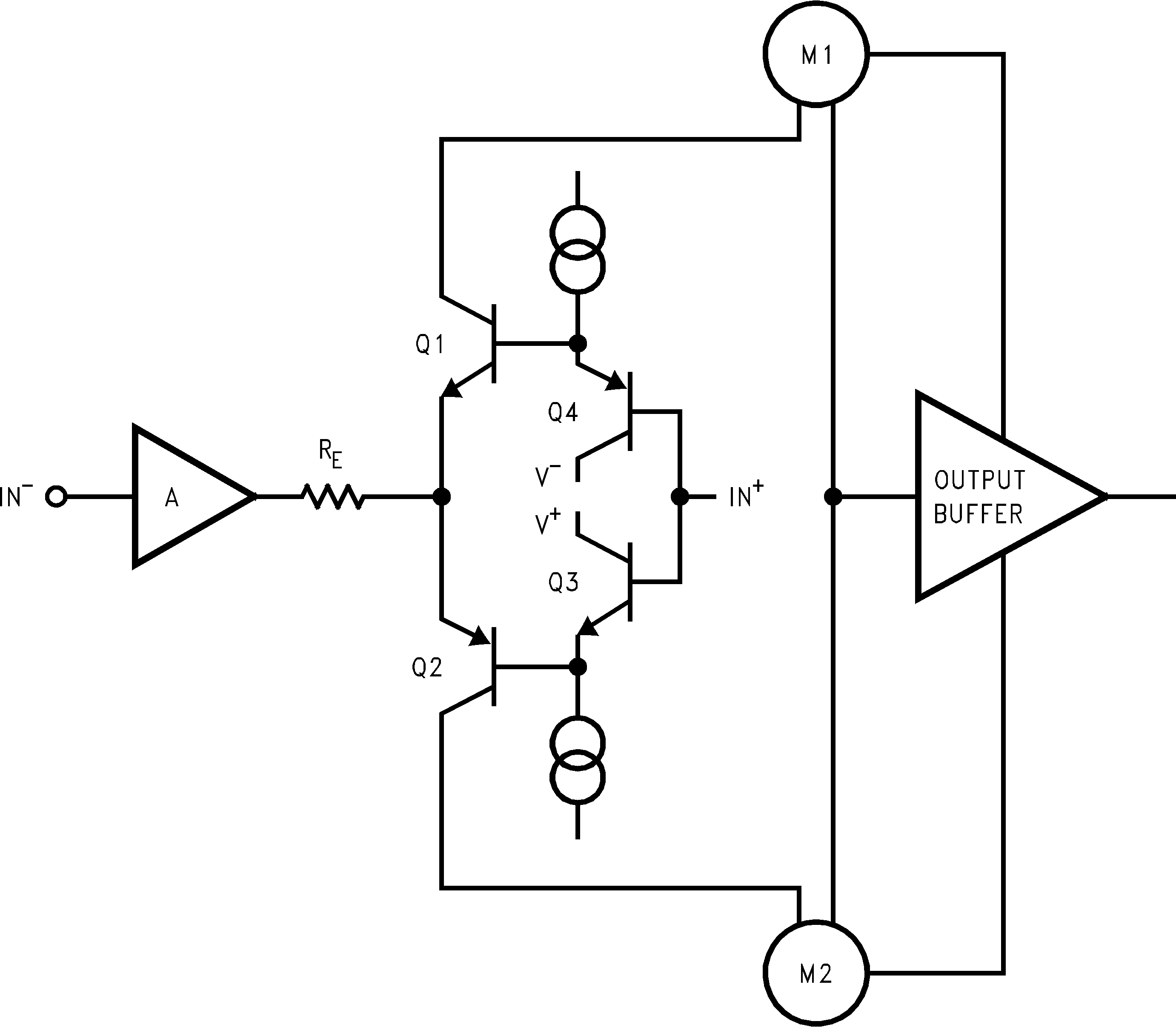
 Simplified Schematic