SNOSAW8E May 2008 – September 2015 LM7321 , LM7322
PRODUCTION DATA.
- 1 Features
- 2 Applications
- 3 Description
- 4 Revision History
- 5 Description continued
- 6 Pin Configuration and Functions
- 7 Specifications
- 8 Detailed Description
- 9 Application and Implementation
- 10Power Supply Recommendations
- 11Layout
- 12Device and Documentation Support
- 13Mechanical, Packaging, and Orderable Information
Package Options
Mechanical Data (Package|Pins)
Thermal pad, mechanical data (Package|Pins)
Orderable Information
9 Application and Implementation
NOTE
Information in the following applications sections is not part of the TI component specification, and TI does not warrant its accuracy or completeness. TI’s customers are responsible for determining suitability of components for their purposes. Customers should validate and test their design implementation to confirm system functionality.
9.1 Application Information
9.1.1 Similar High-Output Devices
The LM7332 is a dual rail-to-rail amplifier with a slightly lower GBW capable of sinking and sourcing 100 mA. It is available in SOIC and VSSOP packages.
The LM4562 is dual op amp with very low noise and 0.7-mV voltage offset.
The LME49870 and LME49860 are single and dual low-noise amplifiers that can work from ±22-V supplies.
9.1.2 Other High Performance SOT-23 Ampliers
The LM7341 is a 4-MHz rail-to-rail input and output part that requires only 0.6 mA to operate, and can drive unlimited capacitive load. It has a voltage gain of 97 dB, a CMRR of 93 dB, and a PSRR of 104 dB.
The LM6211 is a 20-MHz part with CMOS input, which runs on ±12-V or 24-V single supplies. It has rail-to-rail output and low noise.
The LM7121 has a gain bandwidth of 235 MHz.
Detailed information on these parts can be found at www.ti.com.
9.2 Typical Application
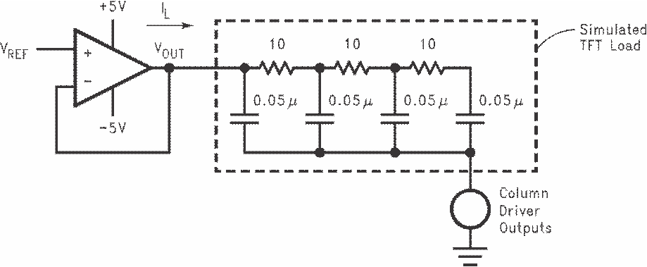
Figure 67 shows a typical application where the LM732xx is used as a buffer amplifier for the VCOM signal employed in a TFT LCD flat panel:
 Figure 67. VCOM Driver Application Schematic
9.2.1 Design Requirements
For this example application, the supply voltage is +5 V, and noninverting gain is necessary.
9.2.2 Detailed Design Procedure
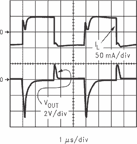
Figure 68 shows the time domain response of the amplifier when used as a VCOM buffer/driver with VREF at ground. In this application, the op amp loop will try and maintain its output voltage based on the voltage on its noninverting input (VREF) despite the current injected into the TFT simulated load. As long as this load current is within the range tolerable by the LM732xx (45-mA sourcing and 65-mA sinking for ±5-V supplies), the output will settle to its final value within less than 2 μs.
 Figure 68. VCOM Driver Performance Scope Photo
9.2.3 Application Curve
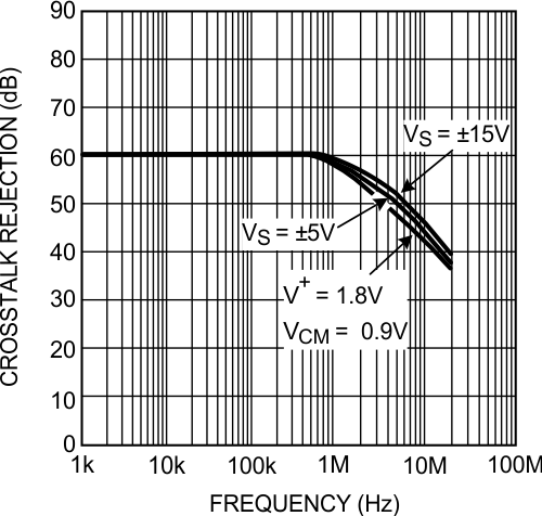
 Figure 69. Crosstalk Rejection vs. Frequency