SNVSAH5A September 2017 – May 2020 LM73605 , LM73606
PRODUCTION DATA.
- 1 Features
- 2 Applications
- 3 Description
- 4 Revision History
- 5 Pin Configuration and Functions
- 6 Specifications
-
7 Detailed Description
- 7.1 Overview
- 7.2 Functional Block Diagram
- 7.3
Feature Description
- 7.3.1 Synchronous Step-Down Regulator
- 7.3.2 Auto Mode and FPWM Mode
- 7.3.3 Fixed-Frequency Peak Current-Mode Control
- 7.3.4 Adjustable Output Voltage
- 7.3.5 Enable and UVLO
- 7.3.6 Internal LDO, VCC_UVLO, and BIAS Input
- 7.3.7 Soft Start and Voltage Tracking
- 7.3.8 Adjustable Switching Frequency
- 7.3.9 Frequency Synchronization and Mode Setting
- 7.3.10 Internal Compensation and CFF
- 7.3.11 Bootstrap Capacitor and VBOOT-UVLO
- 7.3.12 Power-Good and Overvoltage Protection
- 7.3.13 Overcurrent and Short-Circuit Protection
- 7.3.14 Thermal Shutdown
- 7.4 Device Functional Modes
-
8 Application and Implementation
- 8.1 Application Information
- 8.2
Typical Application
- 8.2.1 Design Requirements
- 8.2.2
Detailed Design Procedure
- 8.2.2.1 Custom Design With WEBENCH® Tools
- 8.2.2.2 Output Voltage Setpoint
- 8.2.2.3 Switching Frequency
- 8.2.2.4 Input Capacitors
- 8.2.2.5 Inductor Selection
- 8.2.2.6 Output Capacitor Selection
- 8.2.2.7 Feedforward Capacitor
- 8.2.2.8 Bootstrap Capacitors
- 8.2.2.9 VCC Capacitor
- 8.2.2.10 BIAS
- 8.2.2.11 Soft Start
- 8.2.2.12 Undervoltage Lockout Setpoint
- 8.2.2.13 PGOOD
- 8.2.3 Application Curves
- 9 Power Supply Recommendations
- 10Layout
- 11Device and Documentation Support
- 12Mechanical, Packaging, and Orderable Information
Package Options
Mechanical Data (Package|Pins)
- RNP|30
Thermal pad, mechanical data (Package|Pins)
- RNP|30
Orderable Information
8.2 Typical Application
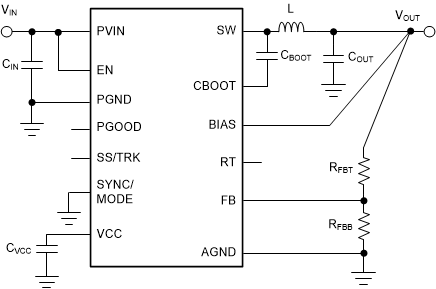
The LM73605 and LM73606requires only a few external components to perform high-efficiency power conversion, as shown in Figure 25.
 Figure 25. LM73605 and LM73606 Basic Schematic
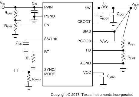
 The LM73605 and LM73606 also integrate many practical features to meet a wide range of system design requirements and optimization, such as UVLO, programmable soft-start time, start-up tracking, programmable switching frequency, clock synchronization, and a power-good flag. Note that for ease of use, the feature pins do not require an additional component when not in use. They can be either left floating or shorted to ground. Please refer to the Pin Configuration and Functions for details.
A comprehensive schematic with all features utilized is shown in Figure 26.
 Figure 26. LM73605 and LM73606 Comprehensive Schematic with All Features Utilized
 The external components must fulfill not only the needs of the power conversion, but also the stability criteria of the control loop. The LM73605 and LM73606are optimized to work with a range of external components. For quick component selection, Table 3 can be used.
Table 3. Typical Component Selection
| fSW (kHz) | VOUT (V) | L (µH) | COUT (µF)(1) | RFBT (kΩ) | RFBB (kΩ) | RT (kΩ) |
| 350 | 1 | 2.2 | 500 | 100 | OPEN | 115 |
| 500 | 1 | 1.5 | 400 | 100 | OPEN | 78.7 or open |
| 1000 | 1 | 0.68 | 200 | 100 | OPEN | 39.2 |
| 2200 | 1 | 0.47 | 100 | 100 | OPEN | 17.4 |
| 350 | 3.3 | 4.7 | 200 | 100 | 43.5 | 115 |
| 500 | 3.3 | 3.3 | 150 | 100 | 43.5 | 78.7 or open |
| 1000 | 3.3 | 1.8 | 88 | 100 | 43.5 | 39.2 |
| 2200 | 3.3 | 1.2 | 44 | 100 | 43.5 | 17.4 |
| 350 | 5 | 6.8 | 120 | 100 | 25 | 115 |
| 500 | 5 | 4.7 | 88 | 100 | 25 | 78.7 or open |
| 1000 | 5 | 3.3 | 66 | 100 | 25 | 39.2 |
| 2200 | 5 | 2.2 | 44 | 100 | 25 | 17.4 |
| 350 | 12 | 15 | 66 | 100 | 9.1 | 115 |
| 500 | 12 | 10 | 44 | 100 | 9.1 | 78.7 or open |
| 1000 | 12 | 6.8 | 22 | 100 | 9.1 | 39.2 |
| 350 | 24 | 22 | 40 | 100 | 4.3 | 115 |
| 500 | 24 | 15 | 30 | 100 | 4.3 | 78.7 or open |