SNOS926F May 1999 – September 2014 LM7372
PRODUCTION DATA.
- 1 Features
- 2 Applications
- 3 Description
- 4 Revision History
- 5 Pin Configuration and Functions
- 6 Specifications
- 7 Typical Performance Characteristics
- 8 Detailed Description
- 9 Application and Implementation
- 10Power Supply Recommendations
- 11Layout
- 12Device and Documentation Support
- 13Mechanical, Packaging, and Orderable Information
Package Options
Refer to the PDF data sheet for device specific package drawings
Mechanical Data (Package|Pins)
- DDA|8
- D|16
Thermal pad, mechanical data (Package|Pins)
- DDA|8
Orderable Information
9 Application and Implementation
NOTE
Information in the following applications sections is not part of the TI component specification, and TI does not warrant its accuracy or completeness. TI’s customers are responsible for determining suitability of components for their purposes. Customers should validate and test their design implementation to confirm system functionality.
9.1 Application Information
The LM7372 is a high speed dual operational amplifier with a very high slew rate and very low distortion. Like many other op amps, it is used in conventional voltage feedback amplifier applications, and has a class AB output stage in order to deliver high currents to low impedance loads. However, it draws a low quiescent supply current in most situations since the supply current increases when necessary to keep up with large output swing and/or high frequency (see High Frequency/Large Signal Swing Considerations). For most op amps in typical applications, this topology means that internal power dissipation is rarely an issue, even with the trend to smaller surface mount packages. However, TI has designed the LM7372 for applications where there are significant levels of power dissipation, and a way to effectively remove the internal heat generated by this power dissipation is needed in order to maintain the semiconductor junction temperature at acceptable levels. This is particularly important in environments with elevated ambient temperatures.
9.2 Typical Application
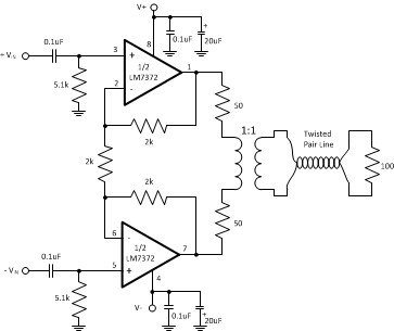 Figure 23. Split Supply Application (SO PowerPAD)
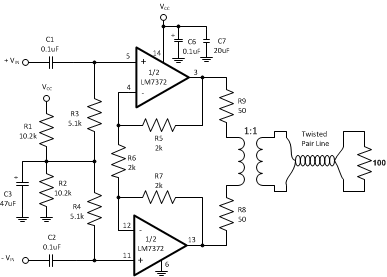 Figure 24. Single Supply Application (16-Pin SOIC)
9.3 Application Details
Several factors contribute to power dissipation and consequently higher semiconductor junction temperatures. Understanding these factors is necessary if the LM7372 is to perform to the desired specifications. Since different applications will have different dissipation levels and since there are various possible compromises between the ways these factors will contribute to the total junction temperature, this section will examine the typical application shown in Figure 24 as an example, and offer solutions when encountering excessive junction temperatures.
There are two major contributors to the internal power dissipation. The first is the product of the supply voltage and the LM7372 quiescent current when no signal is being delivered to the external load, and the second is the additional power dissipated while delivering power to the external load. For low frequency (<1MHz) applications, the LM7372 supply current specification will suffice to determine the quiescent power dissipation (see High Frequency/Large Signal Swing Considerations for cases where the frequency range exceeds 1MHz and the LM7372 supply current increases). The LM7372 quiescent supply current is given as 6.5 mA per amplifier, so with a 24-V supply, the power dissipation is:
where
- (VS = V+ - V−)
This is already a high level of internal power dissipation, and in a small surface mount package with a thermal resistance of RθJA = 140°C/Watt -- a not unreasonable value for an 8-Pin SOIC package -- would result in a junction temperature 140°C/W x 0.312W = 43.7°C above the ambient temperature. A similar calculation using the worst case maximum supply current specification of 8.5 mA per amplifier at an 85°C ambient will yield a power dissipation of 456 mW with a junction temperature of 149°C, perilously close to the maximum permitted junction temperature of 150°C.
The second contributor to high junction temperature is the additional power dissipated internally when power is being delivered to the external load. This cause of temperature rise can be more difficult to calculate, even when the actual operating conditions are known.
For a Class B output stage, one transistor of the output pair will conduct the load current as the output voltage swings positive, with the other transistor drawing no current, and hence dissipating no power. During the other half of the signal swing, this situation is reversed, with the lower transistor sinking the load current and the upper transistor cut off. The current in each transistor will be a half wave rectified version of the total load current. Ideally neither transistor will dissipate power when there is no signal swing, but will dissipate increasing power as the output current increases. However, as the signal voltage across the load increases with load current, the voltage across the output transistor (which is the difference voltage between the supply voltage and the instantaneous voltage across the load) will decrease and a point will be reached where the dissipation in the transistor will begin to decrease again. If the signal is driven into a square wave, ideally the transistor dissipation will fall to zero.
Therefore, for each amplifier, with an effective load each of RL and a sine wave source, integration over the half cycle with a supply voltage VS and a load voltage VL yields the average power dissipation of:
where
- VS is the supply voltage
- VL is the peak signal swing across the load RL
For the package, the power dissipation will be doubled since there are two amplifiers in the package, each contributing half the swing across the load.
The circuit in Single Supply Application, Figure 24, is using the LM7372 as the upstream driver in an ADSL application with Discrete MultiTone modulation. With DMT the upstream signal is spread into 32 adjacent channels each 4 kHz wide. For transmission over POTS, the regular telephone service, this upstream signal from the CPE (Customer Premise Equipment) occupies a frequency band from around 20 kHz up to a maximum frequency of 135 kHz. At first sight, these relatively low transmission frequencies certainly do not seem to require the use of very high speed amplifiers with GBW products in the range of hundreds of megahertz. However, the close spacing of multiple channels places stringent requirements on the linearity of the amplifier, since non-linearities in the presence of multiple tones will cause harmonic products to be generated that can easily interfere with the higher frequency down stream signals also present on the line. The need to deliver 3rd Harmonic distortion terms lower than −75 dBc is the reason for the LM7372 quiescent current levels. Each amplifier is running over 3mA in the output stage alone in order to minimize crossover distortion. The xDSL signal levels are adjusted to provide a given power level on the line, and in the case of ADSL, this is an average power of 13 dBm. For a line with a characteristic impedance of 100 Ω this is only 20 mW (= 1 mW x 10(13/10)). Because the transformer shown in Figure 24 is part of a transceiver circuit, two back-termination resistors are connected in series with each amplifier output. Therefore the equivalent RL for each amplifier is also 100 Ω, and each amplifier is required to deliver 20 mW to this load.
Using Equation 2 with this value for signal swing and a 24V supply, the internal power dissipation per amplifier is 132.8mW. Adding the quiescent power dissipation to the amplifier dissipation gives the total package internal power dissipation as
This result is actually quite pessimistic because it assumes that the dissipation as a result of load current is simply added to the dissipation as a result of quiescent current. This is not correct, since the AB bias current in the output stage is diverted to load current as the signal swing amplitude increases from zero. In fact with load currents in excess of 3.3 mA, all the bias current is flowing in the load, consequently reducing the quiescent component of power dissipation. Also, it assumes a sine wave signal waveform when the actual waveform is composed of many tones of different phases and amplitudes which may demonstrate lower average power dissipation levels.
The average current for a load power of 20 mW is 14.1 mA (= √(20mW/100)). Neglecting the AB bias current, this appears as a full-wave rectified current waveform in the supply current with a peak value of 19.9mA. The peak to average ratio for a waveform of this shape is 1.57, so the total average load current is 12.7 mA (= 19.9 mA/1.57). Adding this to the quiescent current, and subtracting the power dissipated in the load (20 mV x 2 = 40 mW) gives the same package power dissipation level calculated above (= (12.7 + 13) mA x 24 V –40 mV = 576 mW). Nevertheless, when the supply current peak swing is measured, it is found to be significantly lower because the AB bias current is contributing to the load current. The supply current has a peak swing of only 14 mA (compared to 19.9 mA) superimposed on the quiescent current, with a total average value of only 21 mA. Therefore, the total package power dissipation in this application is:
This level of power dissipation would not take the junction temperature in the 8-Pin SO PowerPAD package over the absolute maximum rating at elevated ambient temperatures (barely), but there is no margin to allow for component tolerances or signal variances.
To develop 20 mW in a 100 Ω requires each amplifier to deliver a peak voltage of only 2V, or 4V(P-P). This level of signal swing does not require a high supply voltage but the application uses a 24V supply. This is because the modulation technique uses a large number of tones to transmit the data. While the average power level is held to 20 mW, at any time the phase and amplitude of individual tones will be such as to generate a combined signal with a higher peak value than 2 V. For DMT this crest factor is taken to be around 5.33 so each amplifier has to be able to handle a peak voltage swing of:
If other factors, such as transformer loss or even higher peak to average ratios are allowed for, this means the amplifiers must each swing between 16 to 18 V(P-P).
The required signal swing can be reduced by using a step-up transformer to drive the line. For example a 1:2 ratio will reduce the peak swing requirement by half, and this would allow the supply to be reduced by a corresponding amount. This is not recommended for the LM7372 in this particular application for two reasons. First, although the quiescent power contribution to the overall dissipation is reduced by about 150 mW, the internal power dissipation to drive the load remains the same, since the load for each amplifier is now 25 Ω instead of 100 Ω. Secondly, this is a transceiver application where downstream signals are simultaneously appearing at the transformer secondary. The down stream signals appear differentially across the back termination resistors and are now stepped down by the transformer turns ratio with a consequent loss in receiver sensitivity compared to using a 1:1 transformer. Any trade-off to reduce the supply voltage by an increase in turns ratio should bear these factors in mind, as well as the increased signal current levels required with lower impedance loads.
At an elevated ambient temperature of 85°C and with an average power dissipation of 464mW, a package thermal resistance between 60°C/W and 80°C/W will be needed to keep the maximum junction temperature in the range 110°C to 120°C. The SO PowerPAD package would be the package of choice here with ample board copper area to aid in heat dissipation (see Table 2).
For most standard surface mount packages (8-Pin SOIC, 14-Pin SOIC, 16-Pin SOIC, and so forth), the only means of heat removal from the die is through the bond wires to external copper connecting to the leads. Usually it will be difficult to reduce the thermal resistance of these packages below 100°C/W by these methods and several manufacturers, including Texas Instruments, offer package modifications to enhance the thermal characteristics.
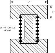 Figure 25. Copper Heatsink Patterns
The LM7372 is available in the 16-Pin SOIC package. Since only 8 pins are needed for the two operational amplifiers, the remaining pins are used for heat sink purposes. Each of the end pins, 1,8,9 & 16 are internally bonded to the lead frame and form an effective means of transferring heat to external copper. This external copper can be either electrically isolated or be part of the topside ground plane in a single supply application.
Figure 25 shows a copper pattern which can be used to dissipate internal heat from the LM7372. Table 1 gives some values of RθJA for different values of L and H with 1oz copper.
Table 1. 16-Pin SOIC Thermal Resistance with Area of Cu
| L (in) | H (in) | RθJA (°C/W) |
|---|---|---|
| 1 | 0.5 | 83 |
| 2 | 1 | 70 |
| 3 | 1.5 | 67 |
From Table 1 it is apparent that two areas of 1oz copper at each end of the package, each 2 in2 in area (for a total of 2600mm2) will be sufficient to hold the maximum junction temperature under 120°C with an 85°C ambient temperature.
An even better package for removing internally generated heat is a package with an exposed die attach paddle. Improved removal of internal heat can be achieved by directly connecting bond wires to the lead frame inside the package. Since this lead frame supports the die attach paddle, heat is transferred directly from the substrate to the outside copper by these bond wires. The LM7372 is also available in the 8-Pin SO PowerPAD package. For this package the entire lower surface of the paddle is not covered with plastic, which would otherwise act as a thermal barrier to heat transfer. Heat is transferred directly from the die through the paddle rather than through the small diameter bonding wires. Values of RθJA in °C/W for the SO PowerPAD package with various areas and weights of copper are tabulated in Table 2.
Table 2. Thermal Resistance of SO PowerPAD Package
| COPPER | AREA | 0.5 in2
(EACH SIDE) |
1.0 in2
(EACH SIDE) |
2.0 in2
(EACH SIDE) |
|---|---|---|---|---|
| 0.5 oz 1.0 oz 2.0 oz |
Top Layer Only |
115 91 74 |
105 79 60 |
102 72 52 |
| 0.5 oz 1.0 oz 2.0 oz |
Bottom Layer Only |
102 92 85 |
88 75 66 |
81 65 54 |
| 0.5 oz 1.0 oz 2.0 oz |
Top And Bottom | 83 71 63 |
70 57 48 |
63 47 37 |
Table 2 clearly demonstrates the superior thermal qualities of the exposed pad package. For example, using the topside copper only in the same way as shown for the SOIC package (Figure 25), the SO PowerPAD requires half the area of 1 oz copper (2 in2, total or 1300mm2), for a comparable thermal resistance of 72°C/Watt. This gives considerably more flexibility in the PCB layout aside from using less copper.
The shape of the heat sink shown in Figure 25 is necessary to allow external components to be connected to the package pins. If thermal vias are used beneath the SO PowerPAD to the bottom side ground plane, then a square pattern heat sink can be used and there is no restriction on component placement on the top side of the board. Even better thermal characteristics are obtained with bottom layer heat sinking. A 2 inch square of 0.5oz copper gives the same thermal resistance (81°C/W) as a competitive thermally enhanced 8-Pin SOIC package which needs two layers of 2 oz copper, each 4 in2 (for a total of 5000 mm2). With heavier copper, thermal resistances as low as 54°C/W are possible with bottom side heat sinking only, substantially improving the long term reliability since the maximum junction temperature is held to less than 110°C, even with an ambient temperature of 85°C. If both top and bottom copper planes are used, the thermal resistance can be brought to under 40°C/W.
9.3.1 High Frequency/Large Signal Swing Considerations
The LM7372 employs a unique input stage in order to support large slew rate and high output current capability with large output swings, with a relatively low quiescent current. This input architecture boosts the device supply current when the application demands it. The result is a supply current which increases at high enough frequencies when the output swing is large enough with added power dissipation as a consequence.
Figure 26 shows the amount of increase in supply current as a function of frequency for various sinusoidal output swing amplitudes:
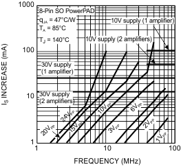 Figure 26. Power Supply Current Increase
Figure 26 shows that there could be 1 mA or more excess supply current per amplifier with close to full output swing (24 VPP) when frequency is just above 1MHz (or at higher frequencies when the output swing is less). This boost in supply current enables the output to “keep up” with high frequency/large signal output swing, but in turn, increases the total package power dissipation and therefore raises the device junction temperature. As a consequence, it is necessary to pay special attention to the package heatsink design for these demanding applications, especially for ones that run at higher supply voltages. For that reason, Figure 26 has the safe operating limits for the 8-Pin SO PowerPAD package -- for example, “30V supply (2 amplifiers)” horizontal line -- superimposed on top of it (with TJ limit of 140°C when operated at 85°C ambient), so that the designer can readily decide whether or not there is need for additional heat sinking.
For example, if the LM7372 is operating similarly to the Figure 24 schematic with a single power supply of 10 V, it is safe to have up to 10 VPP output swing at up to 40 MHz with no additional heat sinking. This is determined by inspecting Figure 24 where the "10 V supply (2 amplifiers)" safe operating limit intercepts the 10 VPP swing graph at around 40 MHz Use the "10 V supply (1 amplifier) safe operating limit in cases where the second amplifier in the LM7372 package does not experience high frequency/high output swing conditions.
At any given “IS increase” value (y axis), the product of frequency and output swing remains essentially constant for all output swing plots. This holds true for the lower frequency range before the plots experience a slope increase. Therefore, if the application example just discussed operates up to 60MHz instead, it is possible to calculate the junction-temperature-limited maximum output swing of 6.7 VPP(= 40 MHz x 10VPP/60 MHz) instead.
Please note that Figure 26 precludes any additional amplifier power dissipation related to load (this topic is discussed below in detail). This load current, if large enough, will reduce the operating frequency/output swing further. It is important to note that the LM7372 can be destroyed if it is allowed to dissipate enough power that compromises its maximum junction temperature limit of 150°C.
With the op amp tied to a load, the device power dissipation consists of the quiescent power due to the supply current flow into the device, in addition to power dissipation due to the load current. The load portion of the power itself could include an average value (due to a DC load current) and an AC component. DC load current would flow if there is an output voltage offset, or the output AC average current is non-zero, or if the op amp operates in a single supply application where the output is maintained somewhere in the range of linear operation. Therefore:
For PAC, (AC Load Power) see Table 3
where:
- IS = Supply Current
- VS = Total Supply Voltage (V+ - V−)
- IO = Average Load Current
- VO = Average Output Voltage
- VR = Reference Voltage (V+ for sourcing and V− for sinking current)
Table 3 shows the maximum AC component of the load power dissipated by the op amp for standard Sinusoidal, Triangular, and Square Waveforms:
Table 3. Normalized Maximum AC Power Dissipated in the Output Stage for Standard Waveforms
| PAC (W.Ω/V2) | ||
|---|---|---|
| SINUSOIDAL | TRIANGULAR | SQUARE |
| 50.7 x 10⁻³ | 46.9 x 10⁻³ | 62.5 x 10⁻³ |
The table entries are normalized to VS2/RL. These entries are computed at the output swing point where the amplifier dissipation is the highest for each waveform type. To figure out the AC load current component of power dissipation, simply multiply the table entry corresponding to the output waveform by the factor VS2/RL. For example, with ±5V supplies, a 100-Ω load and triangular output waveform, power dissipation in the output stage is calculated as: PAC = 46.9 x 10−3 x 102/100 = 46.9mW which contributes another 2.2°C (= 46.9mW x 47°C/W) rise to the LM7372 junction temperature in the 8-Pin SO PowerPAD package.