SLVSFD0 September 2019 LM74202-Q1
PRODUCTION DATA.
- 1 Features
- 2 Applications
- 3 Description
- 4 Revision History
- 5 Pin Configuration and Functions
- 6 Specifications
- 7 Parameter Measurement Information
-
8 Detailed Description
- 8.1 Overview
- 8.2 Functional Block Diagram
- 8.3
Feature Description
- 8.3.1 Undervoltage Lockout (UVLO)
- 8.3.2 Overvoltage Protection (OVP)
- 8.3.3 Reverse Battery Protection
- 8.3.4 Hot Plug-In and In-Rush Current Control
- 8.3.5 Overload and Short Circuit Protection
- 8.4 Device Functional Modes
-
9 Application and Implementation
- 9.1 Application Information
- 9.2
Typical Application
- 9.2.1 Design Requirements
- 9.2.2 Detailed Design Procedure
- 9.2.3 Application Curves
- 10Power Supply Recommendations
- 11Layout
- 12Device and Documentation Support
- 13Mechanical, Packaging, and Orderable Information
Package Options
Mechanical Data (Package|Pins)
- PWP|16
Thermal pad, mechanical data (Package|Pins)
- PWP|16
Orderable Information
8.3.2 Overvoltage Protection (OVP)
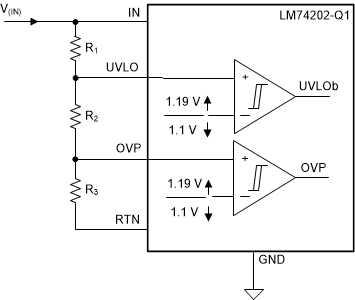
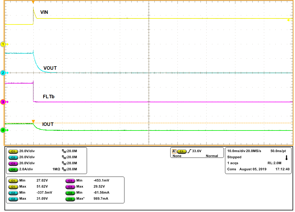
The device incorporates circuitry to protect the system during overvoltage conditions. This device features an overvoltage cut off functionality. A voltage more than V(OVPR) on OVP pin turns off the internal FET and protects the downstream load. To program the OVP threshold, connect a resistor divider from IN supply to OVP terminal to RTN as shown in Figure 21. OVP Overvoltage Cut-off response is shown in Figure 22. OVP pin must not be left floating. If OVP pin could be floating due to dry soldering, an additional zener diode at the output will be required for protection from over voltage.
 Figure 21. OVP Threshold Setting
  Figure 22. OVP Overvoltage Cut-Off
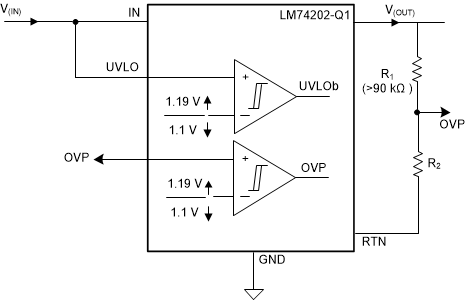
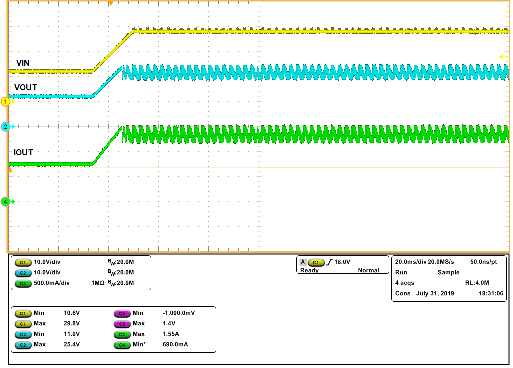
 Programmable overvoltage clamp can also be achieved using LM74202-Q1 by connecting the resistor ladder from Vout to OVP to RTN as shown in Figure 23 . This results in clamping of output voltage close to OVP set-point by resistors R1 and R2. as shown in Figure 24. This scheme will also help in achieving minimal system Iq during off state. For this OVP configurataion, use R1 > 90 kΩ.

 Figure 24. Programmable Overvoltage Clamp Response
 If the OVP pin is connected to GND, the device will clamp the output voltage to 37.5 V (typical).