SLVSFH8B September 2021 – March 2022 LM74720-Q1
PRODUCTION DATA
- 1 Features
- 2 Applications
- 3 Description
- 4 Revision History
- 5 Pin Configuration and Functions
- 6 Specifications
- 7 Parameter Measurement Information
- 8 Detailed Description
-
9 Application and Implementation
- 9.1 Application Information
- 9.2
Typical 12-V Reverse Battery Protection Application
- 9.2.1 Design Requirements for 12-V Battery Protection
- 9.2.2 Automotive Reverse Battery Protection
- 9.2.3
Detailed Design Procedure
- 9.2.3.1 Design Considerations
- 9.2.3.2 Boost Converter Components (C2, C3, L1)
- 9.2.3.3 Input and Output Capacitance
- 9.2.3.4 Hold-Up Capacitance
- 9.2.3.5 Overvoltage Protection and Battery Monitor
- 9.2.3.6 MOSFET Selection: Blocking MOSFET Q1
- 9.2.3.7 MOSFET Selection: Load Disconnect MOSFET Q2
- 9.2.3.8 TVS Selection
- 9.2.4 Application Curves
- 9.3 Do's and Don'ts
- 10Power Supply Recommendations
- 11Layout
- 12Device and Documentation Support
- 13Mechanical, Packaging, and Orderable Information
Package Options
Mechanical Data (Package|Pins)
- DRR|12
Thermal pad, mechanical data (Package|Pins)
- DRR|12
Orderable Information
9.2.3.4 Hold-Up Capacitance
Usually bulk capacitors are placed on the output due to various reasons such as uninterrupted operation during power interruption or micro-short at the input, hold-up requirements for doing a memory dump before turning of the module and filtering requirements as well. This design considers minimum bulk capacitors requirements for meeting functional status "A" during LV124 E10 test case 2 100-µs input interruption. To achieve functional pass status A, acceptable voltage droop in the output of LM74720-Q1 is based on the UVLO settings of downstream DC/DC converters. For this design, a 1-V drop in output voltage for 100 µs is considered and the minimum hold-up capacitance required is calculated by
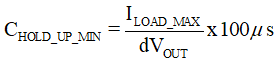
Hold-up capacitance required for 1-V drop in 100 µs is 470 µF.