SLVSFH8B September 2021 – March 2022 LM74720-Q1
PRODUCTION DATA
- 1 Features
- 2 Applications
- 3 Description
- 4 Revision History
- 5 Pin Configuration and Functions
- 6 Specifications
- 7 Parameter Measurement Information
- 8 Detailed Description
-
9 Application and Implementation
- 9.1 Application Information
- 9.2
Typical 12-V Reverse Battery Protection Application
- 9.2.1 Design Requirements for 12-V Battery Protection
- 9.2.2 Automotive Reverse Battery Protection
- 9.2.3
Detailed Design Procedure
- 9.2.3.1 Design Considerations
- 9.2.3.2 Boost Converter Components (C2, C3, L1)
- 9.2.3.3 Input and Output Capacitance
- 9.2.3.4 Hold-Up Capacitance
- 9.2.3.5 Overvoltage Protection and Battery Monitor
- 9.2.3.6 MOSFET Selection: Blocking MOSFET Q1
- 9.2.3.7 MOSFET Selection: Load Disconnect MOSFET Q2
- 9.2.3.8 TVS Selection
- 9.2.4 Application Curves
- 9.3 Do's and Don'ts
- 10Power Supply Recommendations
- 11Layout
- 12Device and Documentation Support
- 13Mechanical, Packaging, and Orderable Information
Package Options
Mechanical Data (Package|Pins)
- DRR|12
Thermal pad, mechanical data (Package|Pins)
- DRR|12
Orderable Information
9.2.3.7 MOSFET Selection: Load Disconnect MOSFET Q2
The VDS rating of the MOSFET Q2 must be sufficient to handle the maximum system voltage along with the input transient voltage. For this 12-V design, transient overvoltage events are during suppressed load dump 35 V 400 ms and ISO 7637-2 pulse 2 A 50 V for 50 µs. Furthermore, ISO 7637-2 Pulse 3B is a very fast repetitive pulse of 100 V 100 ns that is usually absorbed by the input and output ceramic capacitors and the maximum voltage on the 12-V battery can be limited to < 40 V the minimum recommended input capacitance of 0.1 µF. The 50-V SO 7637-2 Pulse 2 A can also be absorbed by input and output capacitors and its amplitude can be reduced to 40-V peak by placing sufficient amount of capacitance at input and output. Choose a MOSFET with ≥ 40-V VDS rating.
The VGS rating of the MOSFET Q2 must be higher than that maximum boost drive output of 15.5 V. FET with VGS absolute maximum rating of +/– 20 VGS is selected.
Inrush current through the MOSFET during input hot-plug into the 12-V battery is determined by output capacitance. External capacitor on PD, CDVDT, is used to limit the inrush current during input hot-plug or startup. The value of inrush current determined by Equation 1 must be selected to ensure that the MOSFET Q2 is operating well within its safe operating area (SOA). To limit inrush current to 1.8-A, value of CDVDT is 10.43 nF, closest standard value of 10.0 nF is chosen.
Duration of inrush current is calculated by:
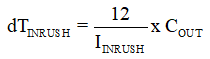
Calculated inrush current duration is 3.13 ms with 1.8-A inrush current.
MOSFET BUK7Y4R8-60E having 60-V VDS and ±20-V VGS rating is selected for Q2. Power dissipation during inrush is well within the MOSFET's safe operating area (SOA).