SNOS808P January 2000 – December 2014 LM75A
PRODUCTION DATA.
- 1 Features
- 2 Applications
- 3 Description
- 4 Revision History
- 5 Pin Configuration and Functions
- 6 Specifications
- 7 Detailed Description
- 8 Application and Implementation
- 9 Power Supply Recommendations
- 10Layout
- 11Device and Documentation Support
- 12Mechanical, Packaging, and Orderable Information
Package Options
Mechanical Data (Package|Pins)
Thermal pad, mechanical data (Package|Pins)
Orderable Information
10 Layout
10.1 Layout Guidelines
To achieve the expected results when measuring temperature with an integrated circuit temperature sensor like the LM75A, it is important to understand that the sensor measures its own die temperature. For the LM75A, the best thermal path between the die and the outside world is through the LM75A's pins. In the VSSOP-8 package, the GND pin is directly connected to the die, so the GND pin provides the best thermal path. If the other pins are at different temperatures (unlikely, but possible), they will affect the die temperature, but not as strongly as the GND pin. In the SOIC-8 package, none of the pins is directly connected to the die, so they will all contribute similarly to the die temperature. Because the pins represent a good thermal path to the LM75A die, the LM75A will provide an accurate measurement of the temperature of the printed circuit board on which it is mounted. There is a less efficient thermal path between the plastic package and the LM75A die. If the ambient air temperature is significantly different from the printed circuit board temperature, it will have a small effect on the measured temperature.
In probe-type applications, the LM75A can be mounted inside a sealed-end metal tube, and can then be dipped into a bath or screwed into a threaded hole in a tank. As with any IC, the LM75A and accompanying wiring and circuits must be kept insulated and dry, to avoid leakage and corrosion. This is especially true if the circuit may operate at cold temperatures where condensation can occur. Printed-circuit coatings and varnishes such as Humiseal and epoxy paints or dips are often used to insure that moisture cannot corrode the LM75A or its connections.
10.1.1 Digital Noise Issues
The LM75A features an integrated low-pass filter on both the SCL and the SDA digital lines to mitigate the effects of bus noise. Although this filtering makes the LM75A communication robust in noisy environments, good layout practices are always recommended. Minimize noise coupling by keeping digital traces away from switching power supplies. Also, ensure that digital lines containing high-speed data communications cross at right angles to the SDA and SCL lines. Excessive noise coupling into the SDA and SCL lines on the LM75A—specifically noise with amplitude greater than 400 mVpp (the LM75A’s typical hysteresis), overshoot greater than 300mV above +Vs, and undershoot more than 300 mV below GND—may prevent successful serial communication with the LM75A. Serial bus no-acknowledge is the most common symptom, causing unnecessary traffic on the bus. Although the serial bus maximum frequency of communication is only 400 kHz, care must be taken to ensure proper termination within a system with long printed circuit board traces or multiple parts on the bus.
10.2 Layout Example
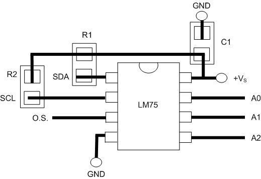 Figure 13. Printed Circuit Board Used for Thermal Resistance Specifications