SNOS808P January 2000 – December 2014 LM75A
PRODUCTION DATA.
- 1 Features
- 2 Applications
- 3 Description
- 4 Revision History
- 5 Pin Configuration and Functions
- 6 Specifications
- 7 Detailed Description
- 8 Application and Implementation
- 9 Power Supply Recommendations
- 10Layout
- 11Device and Documentation Support
- 12Mechanical, Packaging, and Orderable Information
Package Options
Mechanical Data (Package|Pins)
Thermal pad, mechanical data (Package|Pins)
Orderable Information
6 Specifications
6.1 Absolute Maximum Ratings
over operating free-air temperature range (unless otherwise noted)(1)| MIN | MAX | UNIT | |||
|---|---|---|---|---|---|
| Supply Voltage Pin (+VS) | −0.3 | 6.5 | V | ||
| Voltage at A0, A1and A2 Pins | −0.3 | (+VS + 0.3) and must be ≤ 6.5 | V | ||
| Voltage at OS, SCL and SDA Pins | −0.3 | 6.5 | V | ||
| Input Current at any Pin(2) | 5 | mA | |||
| Package Input Current(2) | 20 | mA | |||
| O.S. Output Sink Current | 10 | mA | |||
| O.S. Output Voltage | 6.5 | V | |||
| Storage temperature, Tstg | –65 | 150 | °C | ||
6.2 ESD Ratings
| VALUE | UNIT | |||
|---|---|---|---|---|
| V(ESD) | Electrostatic discharge | Human-body model (HBM), per ANSI/ESDA/JEDEC JS-001(1) | ±2500 | V |
| Charged-device model (CDM), per JEDEC specification JESD22-C101(2) | ±1000 | |||
| Machine model | ±250 | |||
(1) JEDEC document JEP155 states that 500-V HBM allows safe manufacturing with a standard ESD control process.
(2) JEDEC document JEP157 states that 250-V CDM allows safe manufacturing with a standard ESD control process.
6.3 Recommended Operating Conditions(4)(3)
| MIN | MAX | UNIT | |
|---|---|---|---|
| Specified Temperature Range (TMIN to TMAX) | −55 | 125 | °C |
| Supply Voltage Range (+VS) LM75A | 2.7 | 5.5 | V |
6.4 Thermal Information
| THERMAL METRIC(1) | LM75A | UNIT | ||
|---|---|---|---|---|
| D | DGK | |||
| 8 PINS | 8 PINS | |||
| RθJA | Junction-to-ambient thermal resistance | 200 | 250 | °C/W |
(1) For more information about traditional and new thermal metrics, see the IC Package Thermal Metrics application report, SPRA953.
6.5 Temperature-to-Digital Converter Characteristics
Unless otherwise noted, these specifications apply for: +VS = 2.7 to 5.5 Vdc for LM75AIM. TA = TJ = 25°C, unless otherwise noted.| PARAMETER | TEST CONDITIONS | MIN | TYP(9) | MAX(5) | UNIT | ||
|---|---|---|---|---|---|---|---|
| Accuracy | TA = −25°C to +100°C –55°C ≤ TJ ≤ 125°C |
–2 | 2 | °C | |||
| TA = −55°C to +125°C –55°C ≤ TJ ≤ 125°C |
–3 | 3 | |||||
| Resolution | 9 | Bits | |||||
| Temperature Conversion Time | See(6) | 100 | ms | ||||
| See(6), –55°C ≤ TJ ≤ 125°C | 300 | ||||||
| Quiescent Current | LM75A | I2C Inactive | 0.28 | mA | |||
| I2C Inactive, –55°C ≤ TJ ≤ 125°C | 0.5 | ||||||
| Shutdown Mode, +VS = 3 V | 4 | μA | |||||
| Shutdown Mode, +VS = 5 V | 6 | μA | |||||
| O.S. Output Saturation Voltage | IOUT = 4 mA, –55°C ≤ TJ ≤ 125°C | 0.8 | V | ||||
| O.S. Delay | See(7), –55°C ≤ TJ ≤ 125°C | 1 | 6 | Conversion | |||
| TOS Default Temperature | See(8) | 80 | °C | ||||
| THYST Default Temperature | See(8) | 75 | °C | ||||
6.6 Digital DC Characteristics
Unless otherwise noted, these specifications apply for +VS = 2.7 to 5.5 Vdc for LM75AIM and LM75AIMM. TA = TJ = 25°C, unless otherwise noted.| PARAMETER | TEST CONDITIONS | MIN | TYP(9) | MAX(5) | UNIT | ||
|---|---|---|---|---|---|---|---|
| VIN(1) | Logical “1” Input Voltage | –55°C ≤ TJ ≤ 125°C | +VS × 0.7 | +VS + 0.3 | V | ||
| V | |||||||
| VIN(0) | Logical “0” Input Voltage | –55°C ≤ TJ ≤ 125°C | −0.3 | +VS × 0.3 | V | ||
| V | |||||||
| IIN(1) | Logical “1” Input Current | VIN = +VS | 0.005 | μA | |||
| VIN = +VS, –55°C ≤ TJ ≤ 125°C | 1.0 | ||||||
| IIN(0) | Logical “0” Input Current | VIN = 0 V | −0.005 | μA | |||
| VIN = 0 V, –55°C ≤ TJ ≤ 125°C | −1.0 | ||||||
| CIN | All Digital Inputs | 5 | pF | ||||
| IOH | High Level Output Current Open drain leakage |
LM75A | VOH = 5 V, –55°C ≤ TJ ≤ 125°C | 1 | μA | ||
| VOL | Low Level Output Voltage | IOL = 3 mA, –55°C ≤ TJ ≤ 125°C | 0.4 | V | |||
| tOF | Output Fall Time | CL = 400 pF IO = 3 mA, –55°C ≤ TJ ≤ 125°C | 250 | ns | |||
6.7 I2C Digital Switching Characteristics
Unless otherwise noted, these specifications apply for +VS = 2.7 to 5.5 Vdc for LM75AIM and LM75AIMM on output lines = 80 pF unless otherwise specified. TA = TJ = 25°C, unless otherwise noted.| PARAMETER | TEST CONDITIONS | MIN | TYP(9) | MAX(5)(11) | UNIT | ||
|---|---|---|---|---|---|---|---|
| t1 | SCL (Clock) Period | –55°C ≤ TJ ≤ 125°C | 2.5 | ns | |||
| t2 | Data in Set-Up Time to SCL High | –55°C ≤ TJ ≤ 125°C | 100 | ns | |||
| t3 | Data Out Stable after SCL Low | –55°C ≤ TJ ≤ 125°C | 0 | ns | |||
| t4 | SDA Low Set-Up Time to SCL Low (Start Condition) | –55°C ≤ TJ ≤ 125°C | 100 | ns | |||
| t5 | SDA High Hold Time after SCL High (Stop Condition) | –55°C ≤ TJ ≤ 125°C | 100 | ns | |||
| tTIMEOUT | SDA Time Low for Reset of Serial Interface(10) | LM75A | 75 | ms | |||
| –55°C ≤ TJ ≤ 125°C | 325 | ||||||
(1) Absolute Maximum Ratings indicate limits beyond which damage to the device may occur. DC and AC electrical specifications do not apply when operating the device beyond its rated operating conditions.
(2) When the input voltage (VI) at any pin exceeds the power supplies (VI < GND or VI > +VS) the current at that pin should be limited to 5mA. The 20mA maximum package input current rating limits the number of pins that can safely exceed the power supplies with an input current of 5mA to four.
(3) Reflow temperature profiles are different for lead-free and non-lead-free packages. Soldering process must comply with Reflow Temperature Profile specifications. Refer to www.ti.com/packaging.(3)
(4) LM75A θJA (thermal resistance, junction-to-ambient) when attached to a printed circuit board with 2 oz. foil similar to the one shown in Thermal Information is summarized in the table below the Operating Ratings table.
(5) Maximum values (limits) are ensured to AOQL (Average Outgoing Quality Level).
(6) The conversion-time specification is provided to indicate how often the temperature data is updated. The LM75A can be accessed at any time and reading the Temperature Register will yield result from the last temperature conversion. When the LM75A is accessed, the conversion that is in process will be interrupted and it will be restarted after the end of the communication. Accessing the LM75A continuously without waiting at least one conversion time between communications will prevent the device from updating the Temperature Register with a new temperature conversion result. Consequently, the LM75A should not be accessed continuously with a wait time of less than 300ms.
(7) O.S. Delay is user programmable up to 6 “over limit” conversions before O.S. is set to minimize false tripping in noisy environments.
(8) Default values set at power up.
(9) Typicals are at TA = 25°C and represent most likely parametric norm.
(10) Holding the SDA line low for a time greater than tTIMEOUT will cause the LM75A to reset SDA to the IDLE state of the serial bus communication (SDA set High).
(11) Timing specifications are tested at the bus input logic levels (Vin(0)=0.3XVA for a falling edge and Vin(1)=0.7XVA for a rising edge) when the SCL and SDA edge rates are similar.
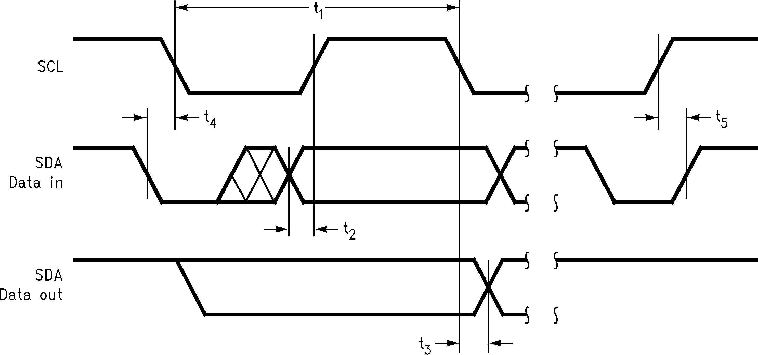 Figure 1. Timing Diagram
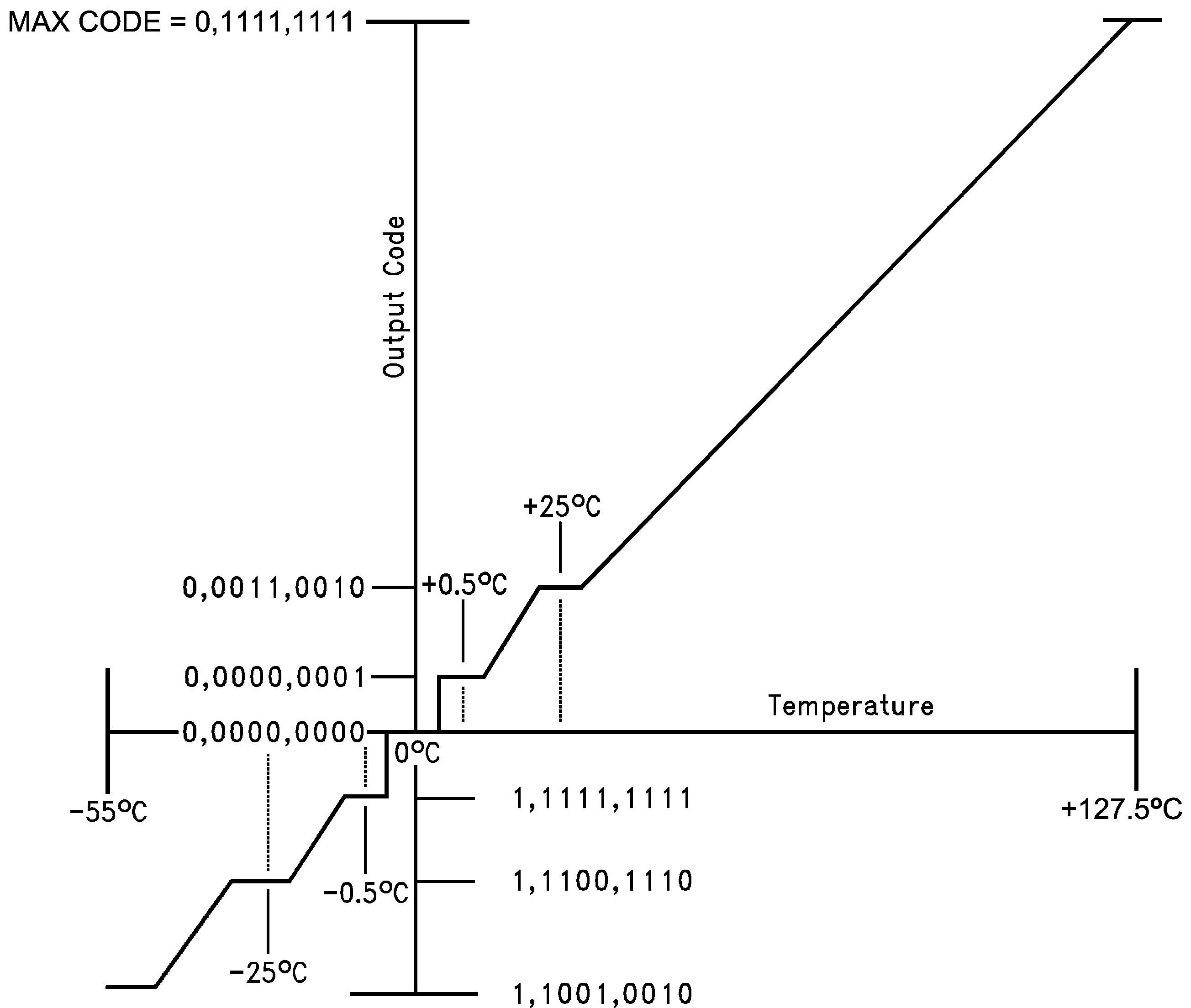 Figure 2. Temperature-to-Digital Transfer Function (Non-Linear Scale for Clarity)
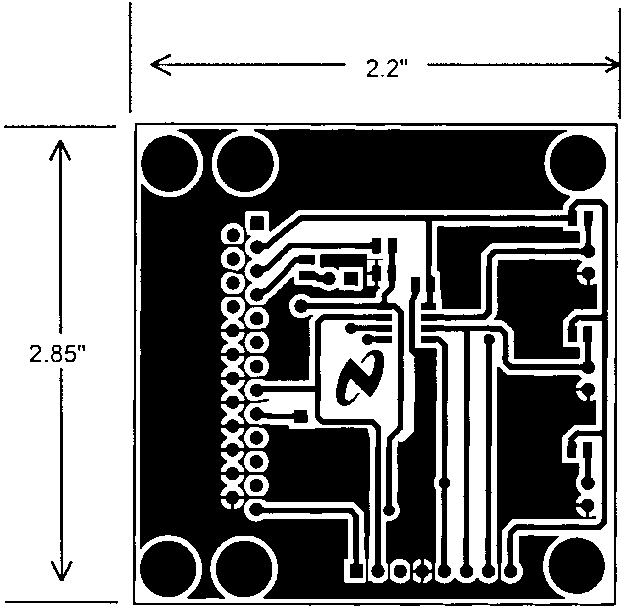 Figure 3. Printed Circuit Board Used for Thermal Resistance Specifications
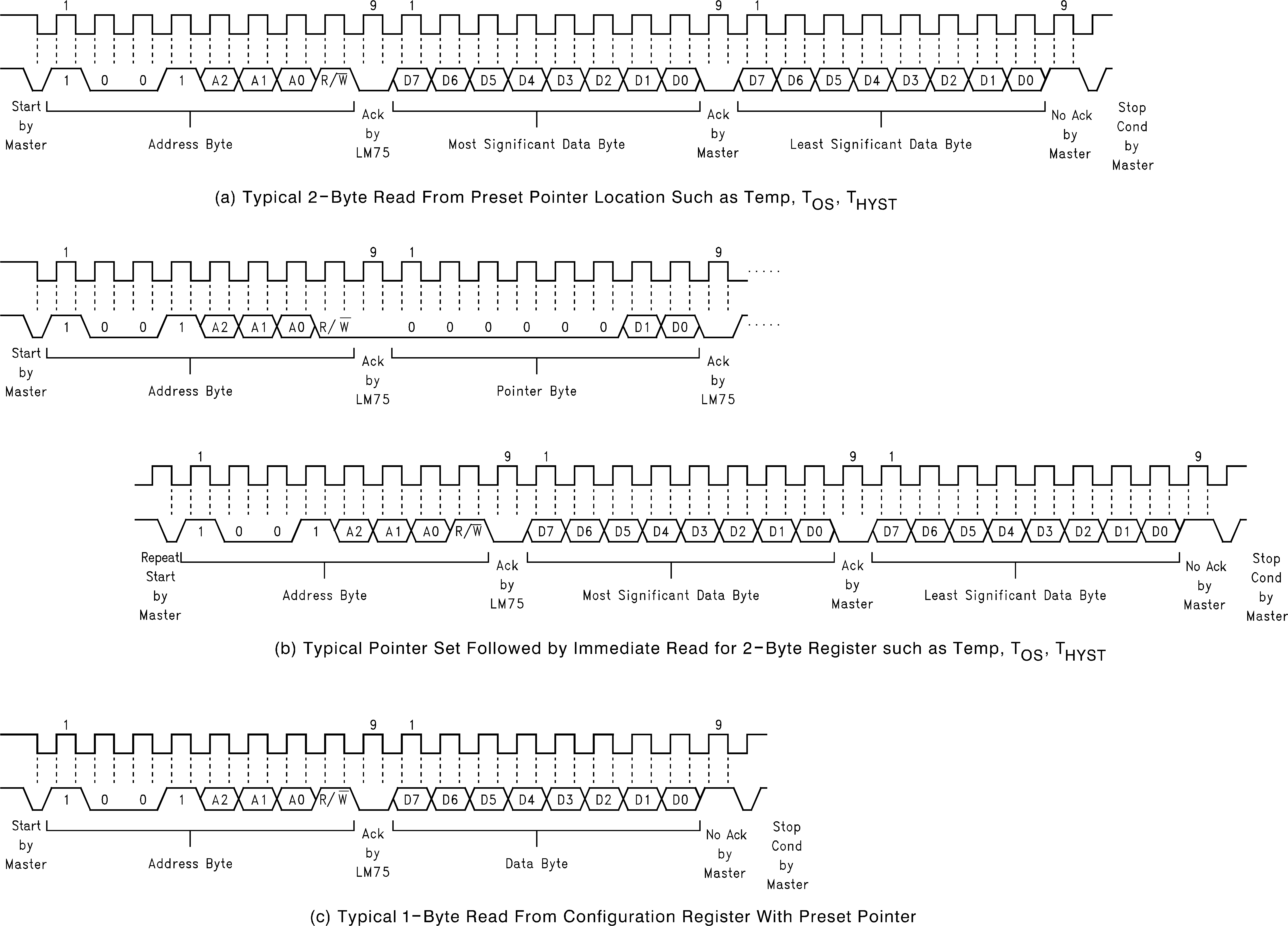 Figure 4. I2C Timing Diagram
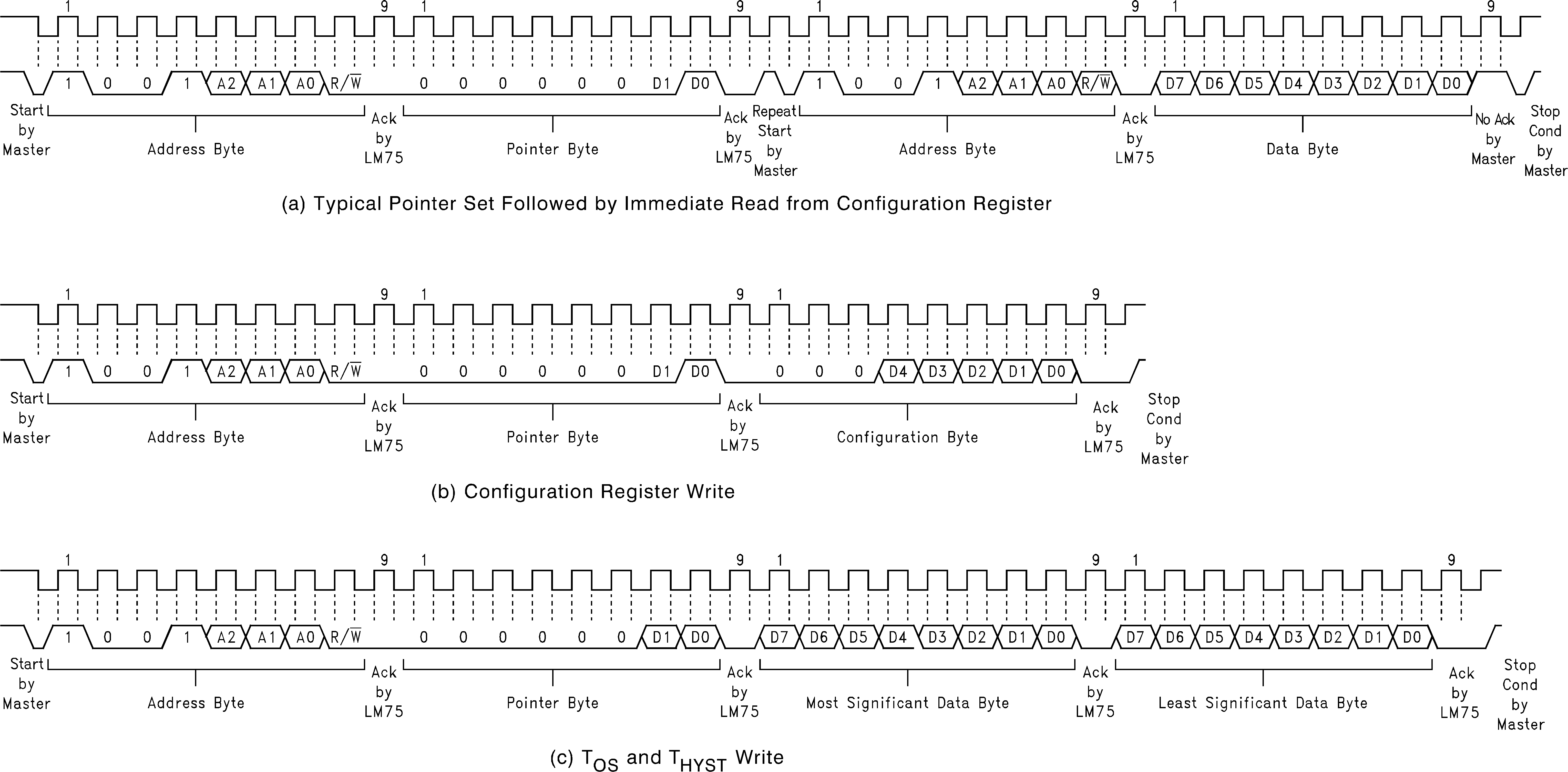 Figure 5. I2C Timing Diagrams (Continued)
6.8 Typical Characteristics
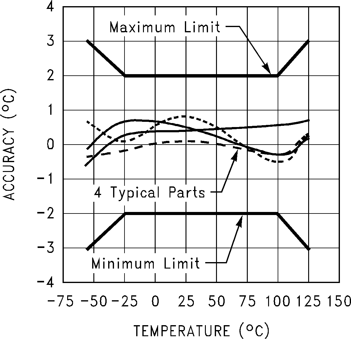 Figure 6. Accuracy vs Temperature (LM75A)