SNOS738I April 1995 – January 2017 LM9061 , LM9061-Q1
PRODUCTION DATA.
- 1 Features
- 2 Applications
- 3 Description
- 4 Revision History
- 5 Pin Configuration and Functions
- 6 Specifications
- 7 Detailed Description
- 8 Application and Implementation
- 9 Power Supply Recommendations
- 10Layout
- 11Device and Documentation Support
- 12Mechanical, Packaging, and Orderable Information
Package Options
Mechanical Data (Package|Pins)
- D|8
Thermal pad, mechanical data (Package|Pins)
Orderable Information
6 Specifications
6.1 Absolute Maximum Ratings
over operating free-air temperature range (unless otherwise noted)(1)(1)| MIN | MAX | UNIT | ||
|---|---|---|---|---|
| Supply voltage | 60 | V | ||
| Output voltage | VCC + 15 | V | ||
| Voltage at sense and threshold (through 1 kΩ) | −25 | 60 | V | |
| ON/OFF input voltage | −0.3 | VCC + 0.3 | V | |
| Reverse supply current | 20 | mA | ||
| Junction temperature | 150 | °C | ||
| Lead temperature soldering, 10 seconds | 260 | °C | ||
| Storage temperature, Tstg | −55 | 150 | °C | |
(1) Stresses beyond those listed under Absolute Maximum Ratings may cause permanent damage to the device. These are stress ratings only, which do not imply functional operation of the device at these or any other conditions beyond those indicated under Recommended Operating Conditions. Exposure to absolute-maximum-rated conditions for extended periods may affect device reliability.
6.2 ESD Ratings: LM9061
| VALUE | UNIT | |||
|---|---|---|---|---|
| V(ESD) | Electrostatic discharge | Human-body model (HBM), per ANSI/ESDA/JEDEC JS-001(1) | ±2000 | V |
| Charged-device model (CDM), per JEDEC specification JESD22-C101(2) | ±1000 | |||
(1) JEDEC document JEP155 states that 500-V HBM allows safe manufacturing with a standard ESD control process.
(2) JEDEC document JEP157 states that 250-V CDM allows safe manufacturing with a standard ESD control process.
6.3 ESD Ratings: LM9061-Q1
| VALUE | UNIT | ||||
|---|---|---|---|---|---|
| V(ESD) | Electrostatic discharge | Human-body model (HBM), per AEC Q100-002(1) | ±2000 | V | |
| Charged-device model (CDM), per AEC Q100-011 | All pins except 1, 4, 5, and 8 | ±1000 | |||
| Pins 1, 4, 5, and 8 | ±1000 | ||||
(1) AEC Q100-002 indicates that HBM stressing shall be in accordance with the ANSI/ESDA/JEDEC JS-001 specification.
6.4 Recommended Operating Conditions(1)
over operating free-air temperature range (unless otherwise noted)| MIN | NOM | MAX | UNIT | ||
|---|---|---|---|---|---|
| Supply voltage | 7 | 26 | V | ||
| ON/OFF input voltage | −0.3 | VCC | V | ||
| Ambient temperature: LM9061 | −40 | 125 | °C | ||
| Junction temperature: LM9061-Q1 | −40 | 125 | °C | ||
(1) Operating Ratings indicate conditions for which the device is intended to be functional, but may not meet the ensured specific performance limits. For ensured specifications and test conditions see the Typical Characteristics.
6.5 Thermal Information
| THERMAL METRIC(1) | LM9061, LM9061-Q1 | UNIT | |
|---|---|---|---|
| D (SOIC) | |||
| 8 PINS | |||
| RθJA | Junction-to-ambient thermal resistance | 150 | °C/W |
| RθJC(top) | Junction-to-case (top) thermal resistance | 46.7 | °C/W |
| RθJB | Junction-to-board thermal resistance | 49.1 | °C/W |
| ψJT | Junction-to-top characterization parameter | 6.2 | °C/W |
| ψJB | Junction-to-board characterization parameter | 48.4 | °C/W |
(1) For more information about traditional and new thermal metrics, see the IC Package Thermal Metrics application report.
6.6 Electrical Characteristics
over operating free-air temperature range (unless otherwise noted)7 V ≤ VCC ≤ 20 V, RREF = 15.4 kΩ, −40°C ≤ TJ ≤ +125°C, unless otherwise specified.
| PARAMETER | TEST CONDITIONS | MIN | TYP | MAX | UNIT | |
|---|---|---|---|---|---|---|
| POWER SUPPLY | ||||||
| IQ | Quiescent supply current | ON/OFF = 0 | 5 | mA | ||
| ICC | Operating supply current | ON/OFF = 1, CLOAD = 0.025 µF, includes turnon transient output current |
40 | mA | ||
| ON/OFF CONTROL INPUT | ||||||
| VIN(0) | ON/OFF input logic 0 | VOUT = OFF | 1.5 | V | ||
| VIN(1) | ON/OFF input logic 1 | VOUT = ON | 3.5 | V | ||
| VHYST | ON/OFF input hysteresis | Peak-to-peak | 0.8 | 2 | V | |
| IIN | ON/OFF input pulldown current | VON/OFF = 5 V | 50 | 250 | µA | |
| GATE DRIVE OUTPUT | ||||||
| VOH | Charge pump output voltage | ON/OFF = 1 | VCC + 7 | VCC + 15 | V | |
| VOL | OFF output voltage | ON/OFF = 0, ISINK = 110 µA | 0.9 | V | ||
| VCLAMP | Sense to output clamp voltage |
ON/OFF = 1, VSENSE = VTHRESHOLD |
11 | 15 | V | |
| ISINK(Normal-OFF) | Output sink current normal operation |
ON/OFF = 0, VDELAY = 0 V, VSENSE = VTHRESHOLD |
75 | 145 | µA | |
| ISINK(Latch-OFF) | Output sink current with protection comparator tripped |
VDELAY = 7 V, VSENSE < VTHRESHOLD |
5 | 15 | µA | |
| PROTECTION CIRCUITRY | ||||||
| VREF | Reference voltage | 1.15 | 1.35 | V | ||
| IREF | Threshold pin reference current | VSENSE = VTHRESHOLD | 75 | 88 | µA | |
| ITHR(LEAKAGE) | Threshold pin leakage current | VCC = Open, 7 V ≤ VTHRESHOLD ≤ 20 V | 10 | µA | ||
| ISENSE | Sense pin input bias current | VSENSE = VTHRESHOLD | 10 | µA | ||
| DELAY TIMER | ||||||
| VTIMER | Delay timer threshold voltage | 5 | 6.2 | V | ||
| VSAT | Discharge transistor saturation voltage | IDIS = 1 mA | 0.4 | V | ||
| IDIS | Delay capacitor discharge current | VDELAY = 5 V | 2 | 10 | mA | |
| IDELAY | Delay pin source current | 6.74 | 15.44 | µA | ||
6.7 Switching Characteristics
over operating free-air temperature range (unless otherwise noted)7V ≤ VCC ≤ 20V, RREF = 15.4 kΩ, −40°C ≤ TJ ≤ +125°C, CLOAD = 0.025 µF, CDELAY = 0.022 µF, unless otherwise specified.
| PARAMETER | TEST CONDITIONS | MIN | TYP | MAX | UNIT | ||
|---|---|---|---|---|---|---|---|
| TON | Output turnon time | CLOAD = 0.025 µF | 7V ≤ VCC ≤ 10 V, VOUT ≥ VCC + 7 V | 1.5 | ms | ||
| 10V ≤ VCC ≤ 20 V, VOUT ≥ VCC + 11 V | 1.5 | ||||||
| TOFF(NORMAL) | Output turnoff time, normal operation(2) |
CLOAD = 0.025 µF VCC = 14 V, VOUT ≥ 25 V VSENSE = VTHRESHOLD |
4 | 10 | ms | ||
| TOFF(Latch-OFF) | Output turnoff time, protection comparator tripped(2) |
CLOAD = 0.025 µF VCC = 14 V, VOUT ≥ 25 V VSENSE = VTHRESHOLD |
45 | 140 | ms | ||
| TDELAY | Delay timer interval | CDELAY = 0.022 µF | 8 | 18 | ms | ||
(1) If Military/Aerospace specified devices are required, please contact the Texas Instruments Sales Office/ Distributors for availability and specifications.
(2) The AC Timing specifications for TOFF are not production tested, and therefore are not specifically ensured. Limits are provided for reference purposes only. Smaller load capacitances will have proportionally faster turn-ON and turn-OFF times.
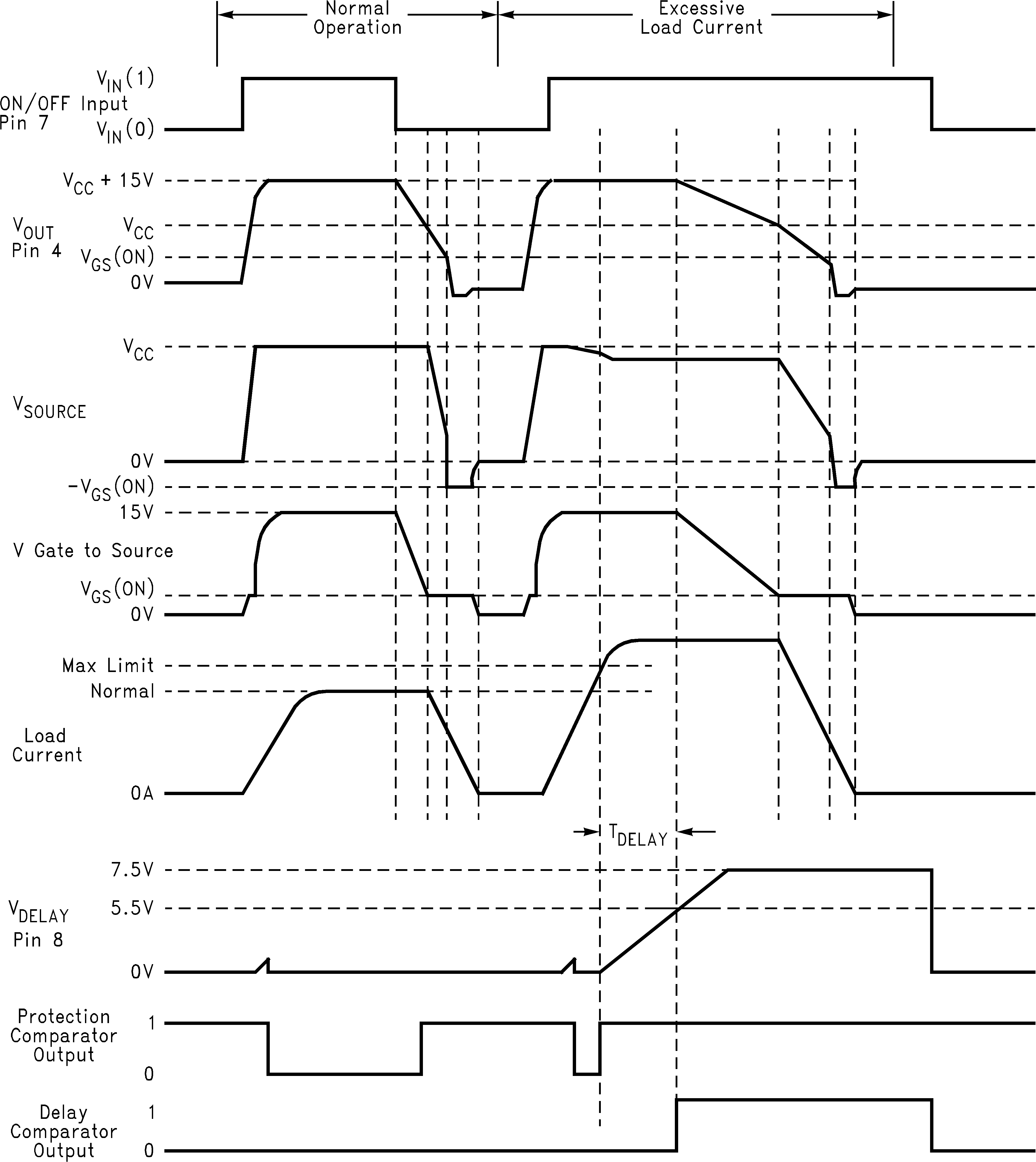 Figure 1. Typical Operating Waveforms
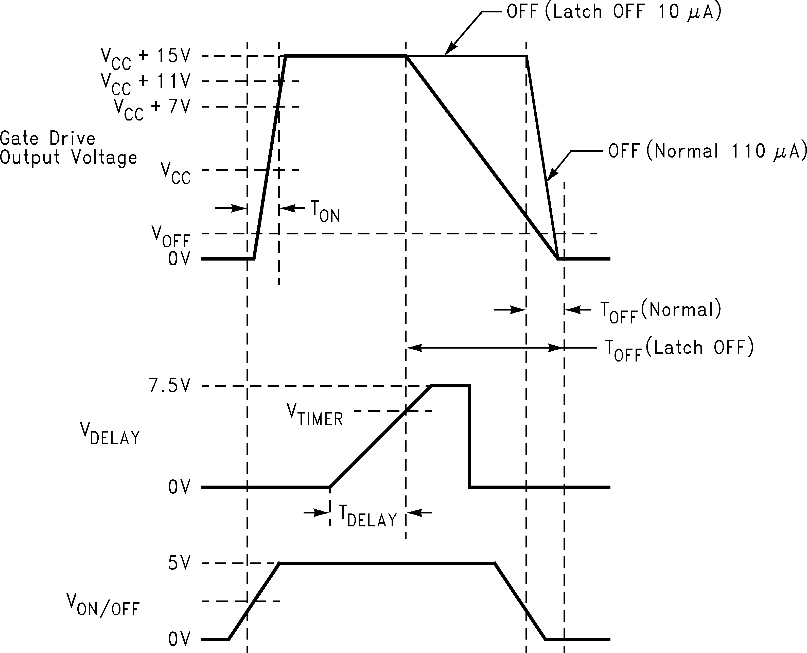 Figure 2. Timing Definitions
6.8 Typical Characteristics
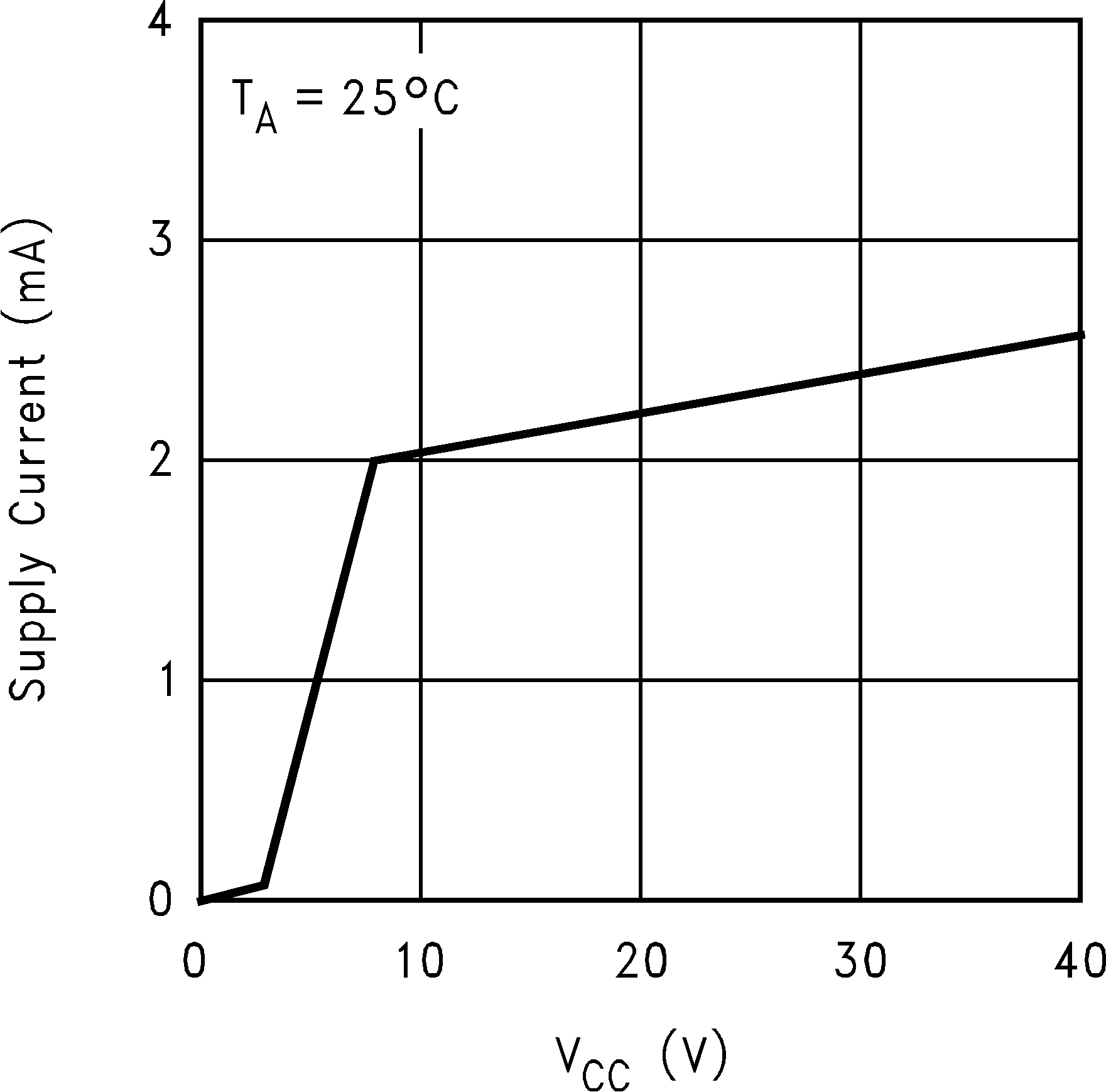 Figure 3. Standby Supply Current vs VCC
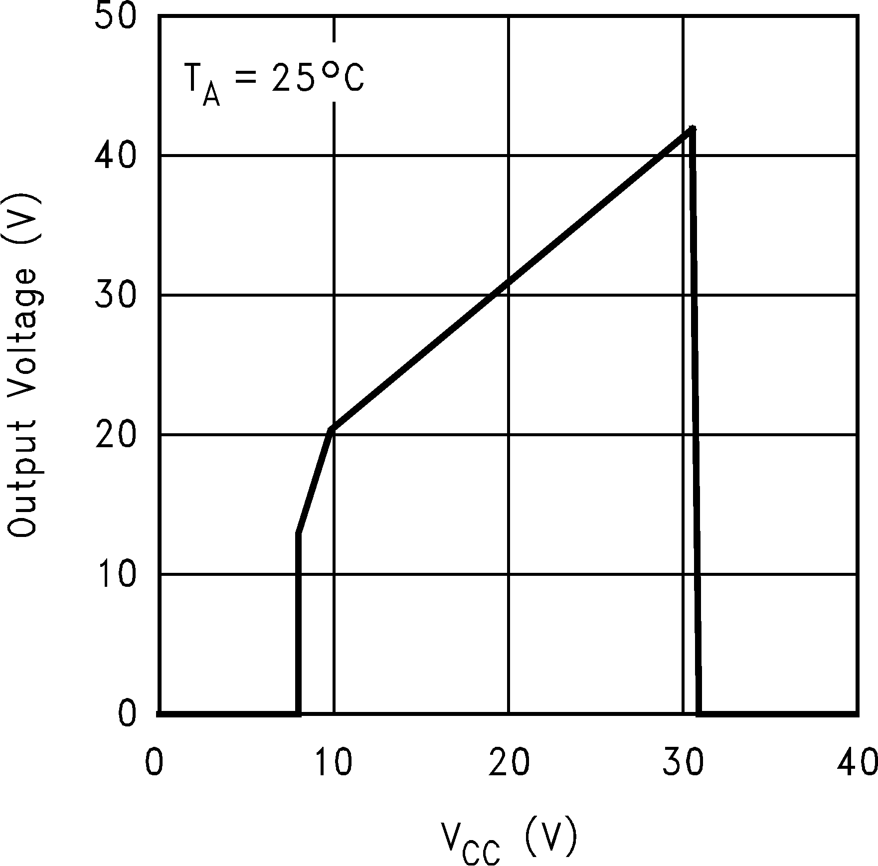 Figure 5. Output Voltage vs VCC
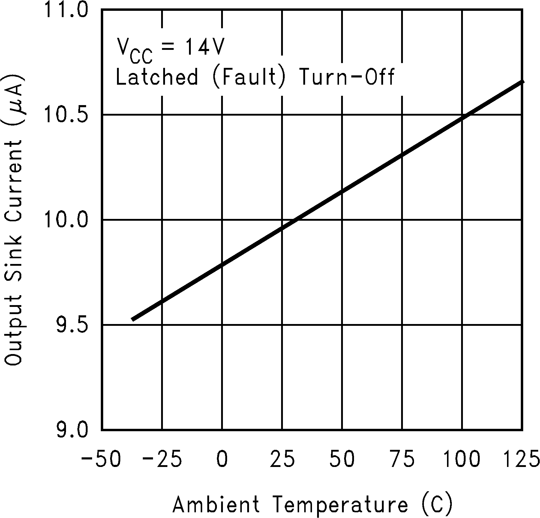 Figure 7. Output Sink Current vs Temperature
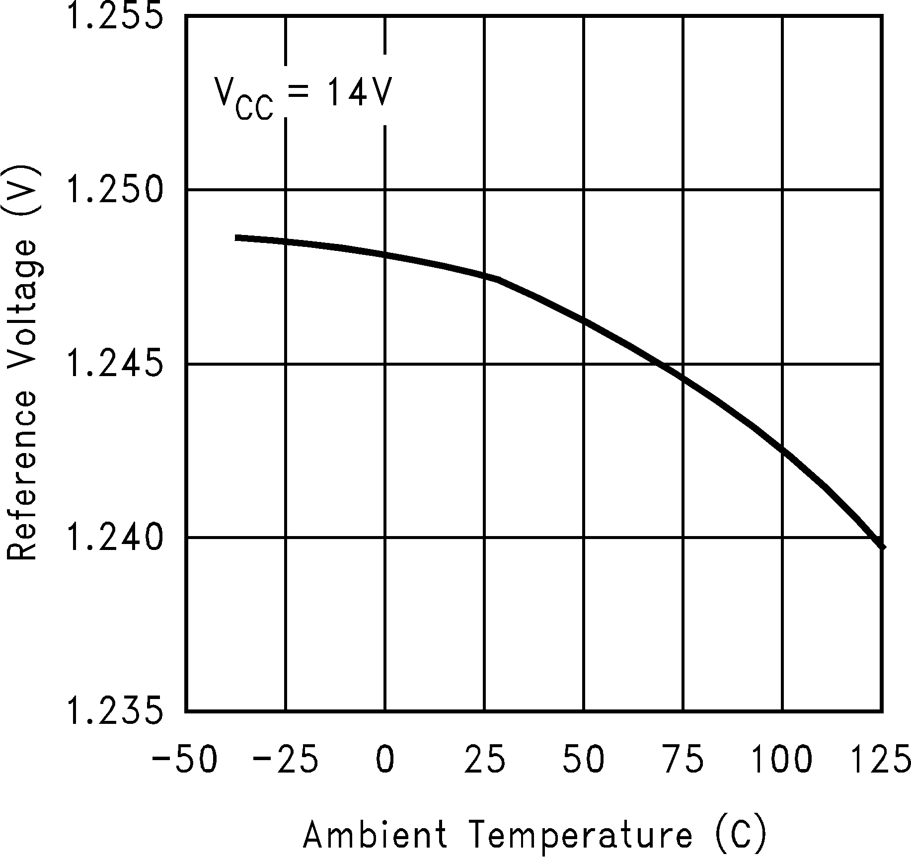 Figure 9. Reference Voltage vs Temperature
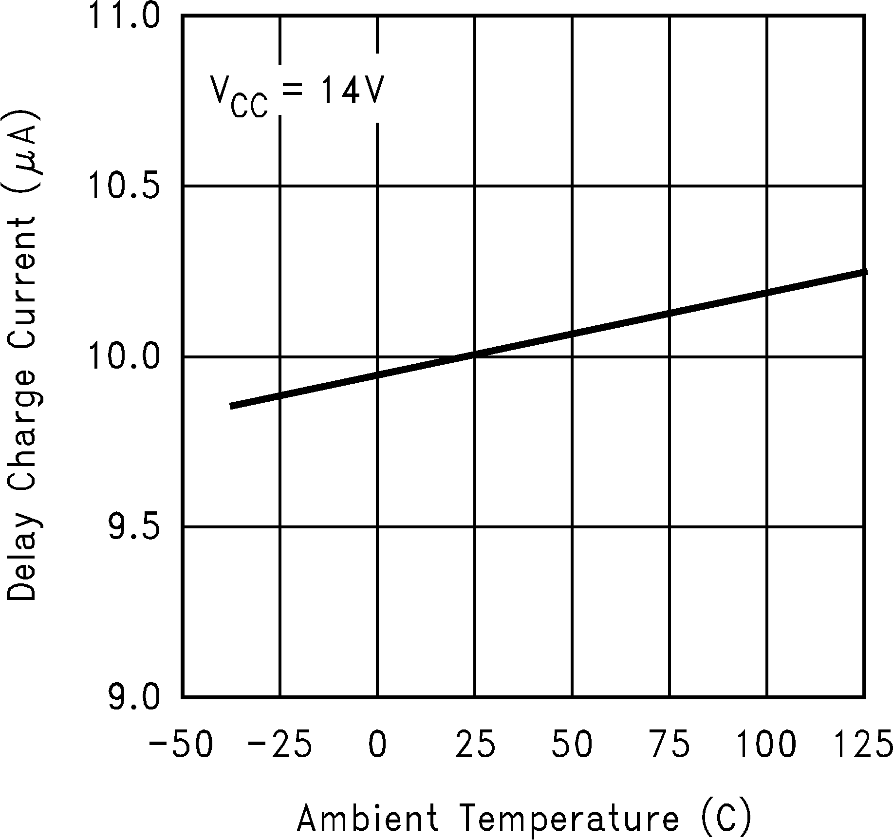 Figure 11. Delay Charge Current vs Temperature
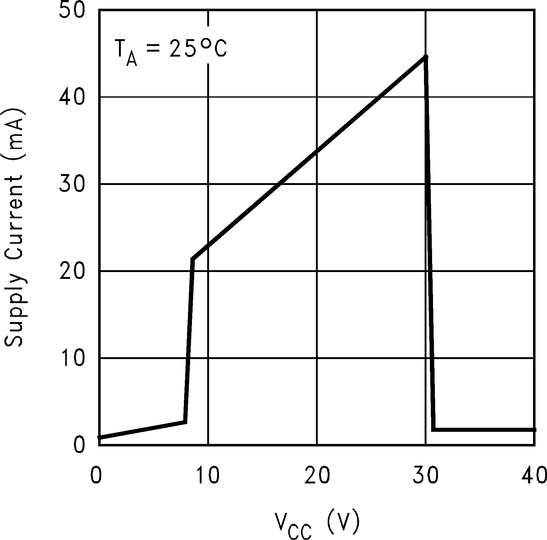 Figure 4. Operating Supply Current vs VCC
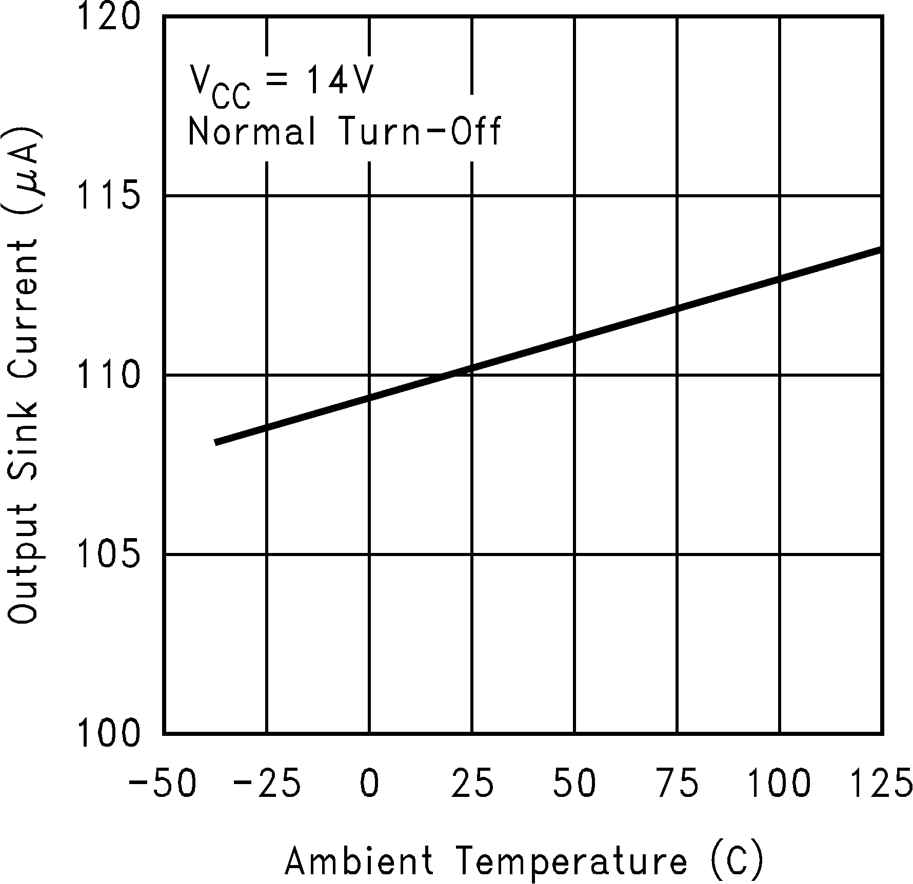 Figure 6. Output Sink Current vs Temperature
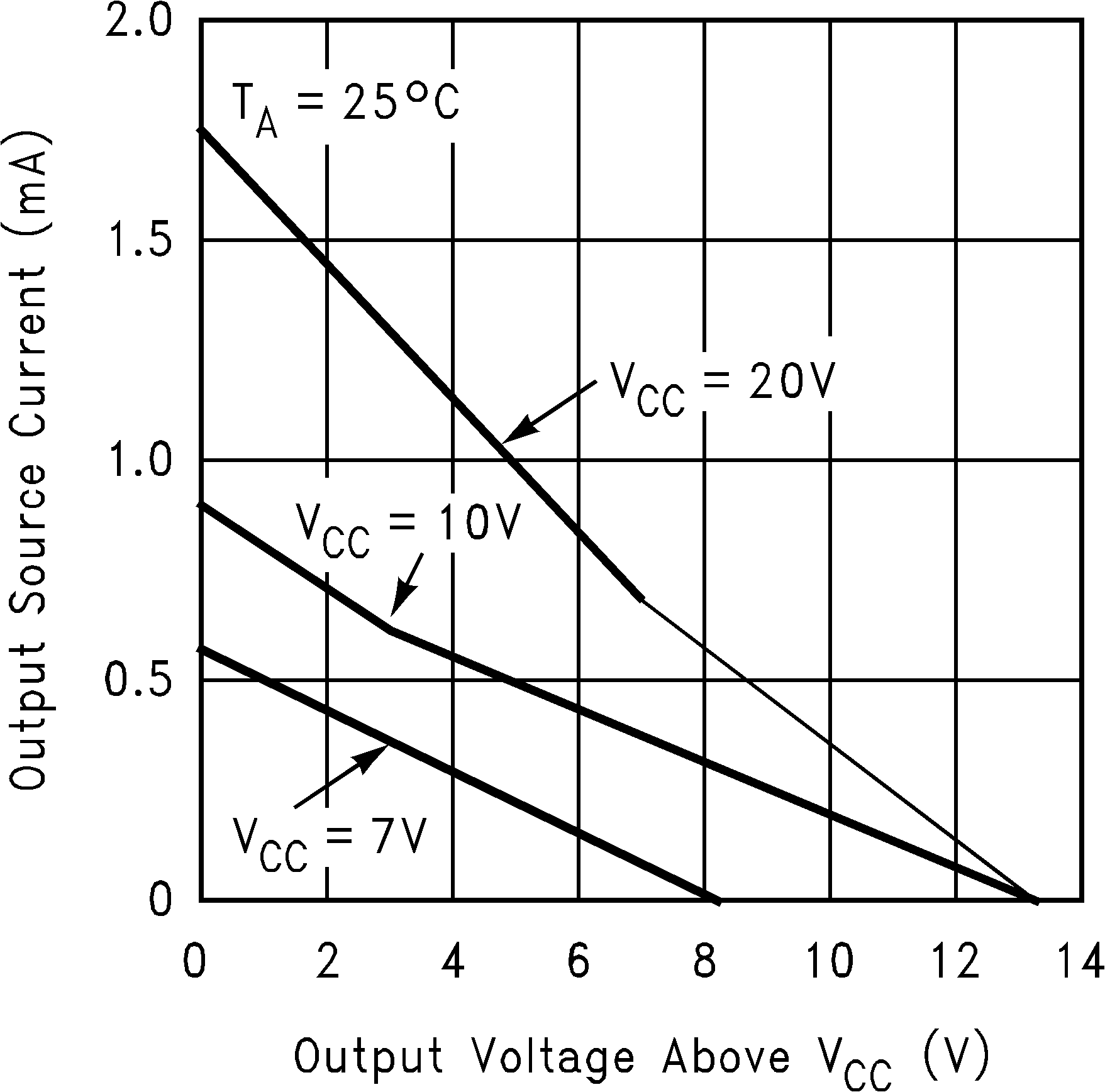 Figure 8. Output Source Current vs Output Voltage
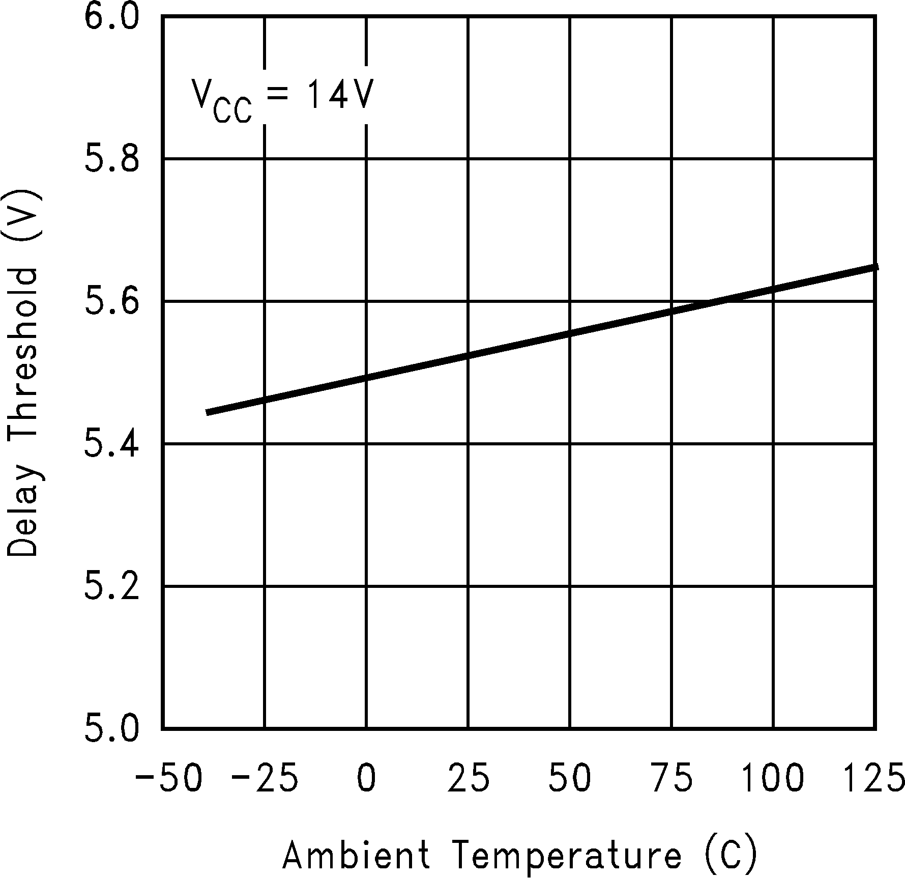 Figure 10. Delay Threshold vs Temperature