SNAS254B October 2006 – April 2017 LM98714
PRODUCTION DATA.
- 1 Features
- 2 Applications
- 3 Description
- 4 Revision History
- 5 Pin Configuration and Functions
- 6 Specifications
-
7 Detailed Description
- 7.1 Overview
- 7.2 Functional Block Diagram
- 7.3
Feature Description
- 7.3.1 Input Clock Introduction
- 7.3.2
Modes of Operation
- 7.3.2.1 Mode 3 - Three Channel Input/Synchronous Pixel Sampling
- 7.3.2.2 Mode 2 - Two Channel Input/Synchronous Pixel Sampling
- 7.3.2.3 Mode 1a - One Channel Input/One, Two, Three, Four, or Five Color Sequential Line Sampling
- 7.3.2.4 Mode 1b - One Channel Input Per Line/Sequential Line (Input) Sampling/Three Channel Processing
- 7.3.3 Input Bias and Clamping
- 7.3.4 Coarse Pixel Phase Alignment
- 7.3.5 Internal Sample Timing
- 7.3.6 Automatic Black Level Correction Loop
- 7.3.7 Internal Timing Generation
- 7.3.8 CCD Timing Generator Master/Slave Modes
- 7.3.9 LVDS Output Mode
- 7.3.10 CMOS Output Mode
- 7.3.11 CMOS Output Data Latency Diagrams
- 7.4
Device Functional Modes
- 7.4.1 Mode 3 - Three Channel Input/Synchronous Pixel Sampling
- 7.4.2 Mode 2 - Two Channel Input/Synchronous Pixel Sampling
- 7.4.3 Mode 1a - One Channel Input/One, Two, Three, Four, Or Five Color Sequential Line Sampling
- 7.4.4 Mode 1b - One Channel Color Input Per Line/Sequential Line (Input) Sampling/Three Channel Processing
- 7.5 Programming
- 7.6 Register Maps
- 8 Application and Implementation
- 9 Device and Documentation Support
- 10Mechanical, Packaging, and Orderable Information
Package Options
Mechanical Data (Package|Pins)
- DGG|48
Thermal pad, mechanical data (Package|Pins)
Orderable Information
1 Features
- LVDS/CMOS Outputs
- LVDS/CMOS Pixel Rate Input Clock or ADC Input Clock
- CDS or S/H Processing for CCD or CIS Sensors
- Independent Gain/Offset Correction for Each Channel
- Digital Black Level Correction Loop for Each Channel
- Programmable Input Clamp Voltage
- Flexible CCD/CIS Sensor Timing Generator
- Key Specifications
- Maximum Input Level: 1.2 or 2.4 Volt Modes
- (Both with + or – Polarity Option)
- ADC Resolution: 16-Bit
- ADC Sampling Rate: 45 MSPS
- INL: ±23 LSB (Typ)
- Channel Sampling Rate: 15/22.5/30 MSPS
- PGA Gain Steps: 256 Steps
- PGA Gain Range: 0.7 to 7.84x
- Analog DAC Resolution: ±9 Bits
- Analog DAC Range: ±300 mV or ±600 mV
- Digital DAC Resolution: ±6 Bits
- Digital DAC Range: –1024 LSB to + 1008 LSB
- SNR: –74dB (at 0 dB PGA Gain)
- Power Dissipation: 505 mW (LVDS) 610 mW (CMOS)
- Operating Temp: 0 to 70°C
- Supply Voltage: 3.3 V Nominal (3.0 V to 3.6 V Range)
- Maximum Input Level: 1.2 or 2.4 Volt Modes
2 Applications
- Multi-Function Peripherals
- Facsimile Equipment
- Flatbed or Handheld Color Scanners
- High-Speed Document Scanner
3 Description
The LM98714 is a fully integrated, high performance 16-Bit, 45 MSPS signal processing solution for digital color copiers, scanners, and other image processing applications. High-speed signal throughput is achieved with an innovative architecture utilizing Correlated Double Sampling (CDS), typically employed with CCD arrays, or Sample and Hold (S/H) inputs (for Contact Image Sensors and CMOS image sensors). The signal paths utilize 8 bit Programmable Gain Amplifiers (PGA), a ±9-Bit offset correction DAC and independently controlled Digital Black Level correction loops for each input. The PGA and offset DAC are programmed independently allowing unique values of gain and offset for each of the three inputs. The signals are then routed to a 45 MHz high performance analog-to-digital converter (ADC). The fully differential processing channel shows exceptional noise immunity, having a very low noise floor of –74dB. The 16-bit ADC has excellent dynamic performance making the LM98714 transparent in the image reproduction chain.
Device Information(1)
| PART NUMBER | PACKAGE | BODY SIZE (NOM) |
|---|---|---|
| LM98714 | TSSOP (48) | 12.50 mm × 6.1 mm |
- For all available packages, see the orderable addendum at the end of the data sheet.
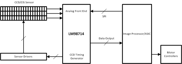
System Block Diagram
