SNOS875H January 2000 – December 2024 LMC6035 , LMC6036
PRODUCTION DATA
- 1
- 1 Features
- 2 Applications
- 3 Description
- 4 Pin Configuration and Functions
- 5 Specifications
- 6 Detailed Description
- 7 Application and Implementation
- 8 Device and Documentation Support
- 9 Revision History
- 10Mechanical, Packaging, and Orderable Information
Package Options
Refer to the PDF data sheet for device specific package drawings
Mechanical Data (Package|Pins)
- D|8
- YAF|8
- DGK|8
- YZR|8
Thermal pad, mechanical data (Package|Pins)
Orderable Information
5.7 Typical Characteristics
at VS = 2.7V, single supply, and TA = 25°C (unless otherwise noted)
 Figure 5-1 Supply Current vs Supply
Voltage (Per Amplifier)
 Figure 5-5 Sourcing Current vs Output
Voltage
 Figure 5-7 Sinking Current vs Output
Voltage
 Figure 5-9 Output Voltage Swing vs Supply
Voltage
 Figure 5-11 Input Noise vs
Frequency
 Figure 5-13 Amp to Amp Isolation vs
Frequency
 Figure 5-15 −PSRR vs
Frequency
 Figure 5-17 Input Offset Voltage vs
Common-Mode Voltage
 Figure 5-19 Input Voltage vs Output
Voltage
 Figure 5-21 Frequency Response vs
Temperature
 Figure 5-23 Gain and Phase vs Capacitive
Load
 Figure 5-25 Non-Inverting Large Signal
Response
 Figure 5-27 Non-Inverting Large Signal
Response
 Figure 5-29 Non-Inverting Small Signal
Response
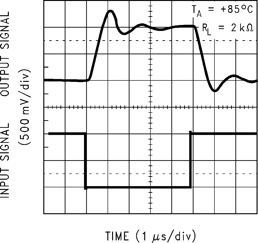
 Figure 5-31 Inverting Large Signal
Response
 Figure 5-33 Inverting Large Signal
Response
 Figure 5-35 Inverting Small Signal
Response
 Figure 5-37 Stability vs Capacitive
Load
 Figure 5-39 Stability vs Capacitive
Load
 Figure 5-41 Stability vs Capacitive
Load
 Figure 5-2 Input Bias Current vs
Temperature
| VS = 15V |
 Figure 5-6 Sourcing Current vs Output
Voltage
 Figure 5-8 Sinking Current vs Output
Voltage
 Figure 5-10 Input Noise vs
Frequency
 Figure 5-12 Amp to Amp Isolation vs
Frequency
 Figure 5-14 +PSRR vs
Frequency
 Figure 5-16 CMRR vs
Frequency
 Figure 5-18 Input Voltage vs Output
Voltage
 Figure 5-20 Frequency Response vs
Temperature
 Figure 5-22 Gain and Phase vs Capacitive
Load
 Figure 5-24 Slew Rate vs Supply
Voltage
 Figure 5-26 Non-Inverting Large Signal
Response
 Figure 5-28 Non-Inverting Small Signal
Response
 Figure 5-30 Non-Inverting Large Signal
Response
 Figure 5-32 Inverting Large Signal
Response
 Figure 5-34 Inverting Small Signal
Response
 Figure 5-36 Inverting Small Signal
Response
 Figure 5-38 Stability vs Capacitive
Load
 Figure 5-40 Stability vs Capacitive
Load
 Figure 5-42 Stability vs Capacitive
Load