SNOS630E August 2000 – February 2024 LMC6081 , LMC6082 , LMC6084
PRODUCTION DATA
- 1
- 1Features
- 2Applications
- 3Description
- 4Pin Configuration and Functions
- 5Specifications
- 6Application and Implementation
- 7Device and Documentation Support
- 8Revision History
- 9Mechanical, Packaging, and Orderable Information
Package Options
Refer to the PDF data sheet for device specific package drawings
Mechanical Data (Package|Pins)
- D|8
- P|8
Thermal pad, mechanical data (Package|Pins)
Orderable Information
6.1.3 Capacitive Load Tolerance
All rail-to-rail output swing op amps have voltage gain in the output stage. A compensation capacitor is normally included in this integrator stage. The frequency location of the dominant pole is affected by the resistive load on the amplifier. Capacitive load driving capability can be optimized by using an appropriate resistive load in parallel with the capacitive load (see Section 5.8).
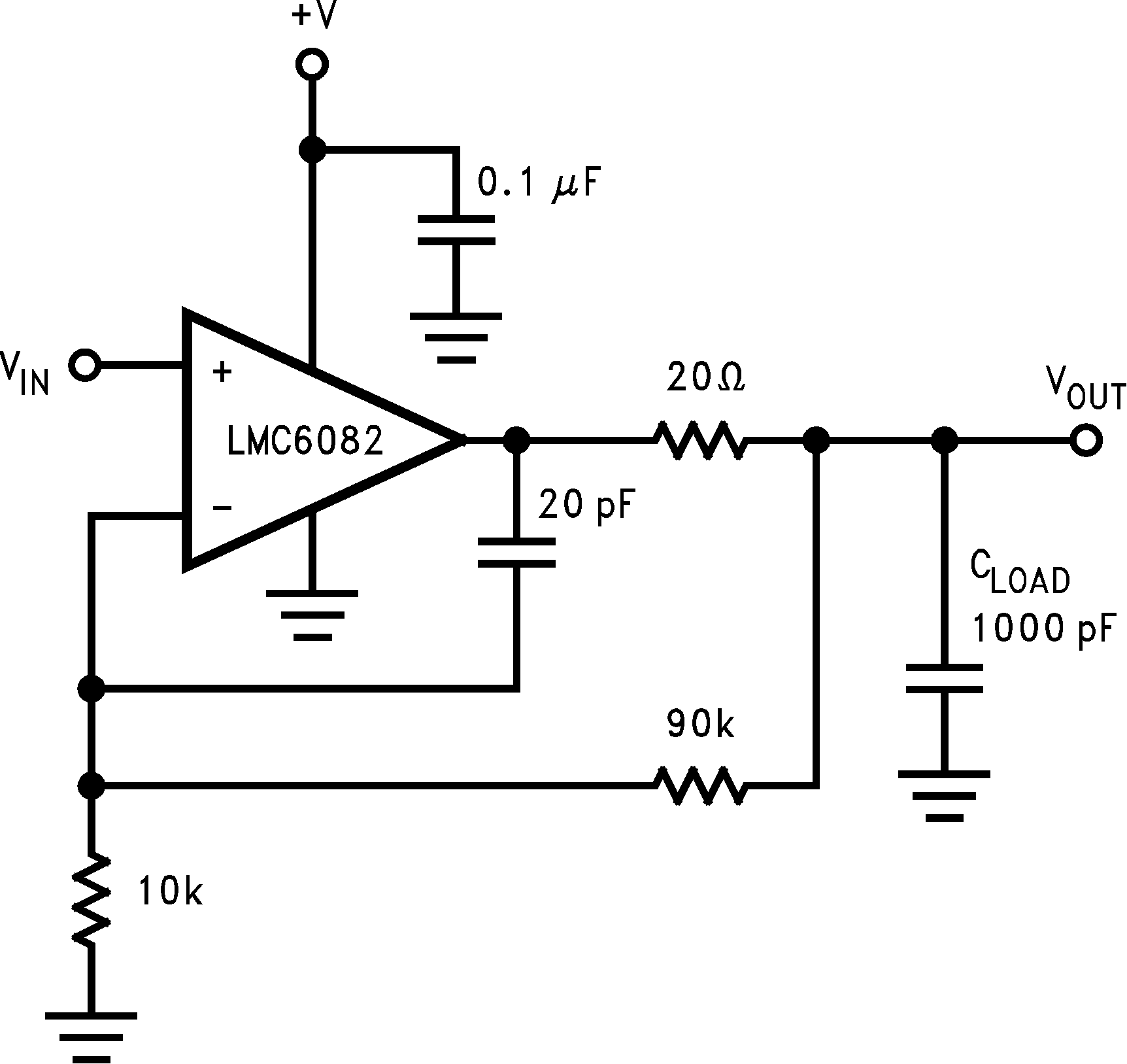
Direct capacitive loading reduces the phase margin of many op amps. A pole in the feedback loop is created by the combination of the op amp output impedance and the capacitive load. This pole induces phase lag at the unity-gain crossover frequency of the amplifier resulting in either an oscillatory or underdamped pulse response. With a few external components, op amps can easily indirectly drive capacitive loads, as shown in Figure 6-2.
 Figure 6-2 LMC6082 Noninverting Gain of 10 Amplifier, Compensated to Handle Capacitive Loads
In the circuit of Figure 6-2, R1 and C1 serve to counteract the loss of phase margin by feeding the high frequency component of the output signal back to the amplifier inverting input, thereby preserving phase margin in the overall feedback loop.
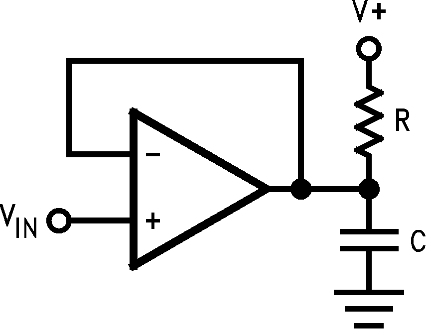
Capacitive load driving capability is enhanced by using a pull up resistor to V+ Figure 6-3. Typically a pull up resistor conducting 500μA or more significantly improves capacitive load responses. The value of the pull up resistor must be determined based on the current sinking capability of the amplifier with respect to the desired output swing. Open loop gain of the amplifier can also be affected by the pullup resistor (see Section 5.7).
 Figure 6-3 Compensating for Large Capacitive Loads With a
Pullup Resistor