SNOSC51D March 1998 – February 2024 LMC660 , LMC662
PRODUCTION DATA
- 1
- 1Features
- 2Applications
- 3Description
- 4Pin Configuration and Functions
- 5Specifications
- 6Application and Implementation
- 7Device and Documentation Support
- 8Revision History
- 9Mechanical, Packaging, and Orderable Information
Package Options
Refer to the PDF data sheet for device specific package drawings
Mechanical Data (Package|Pins)
- D|14
- N|14
Thermal pad, mechanical data (Package|Pins)
Orderable Information
6.1.4 Bias Current Testing
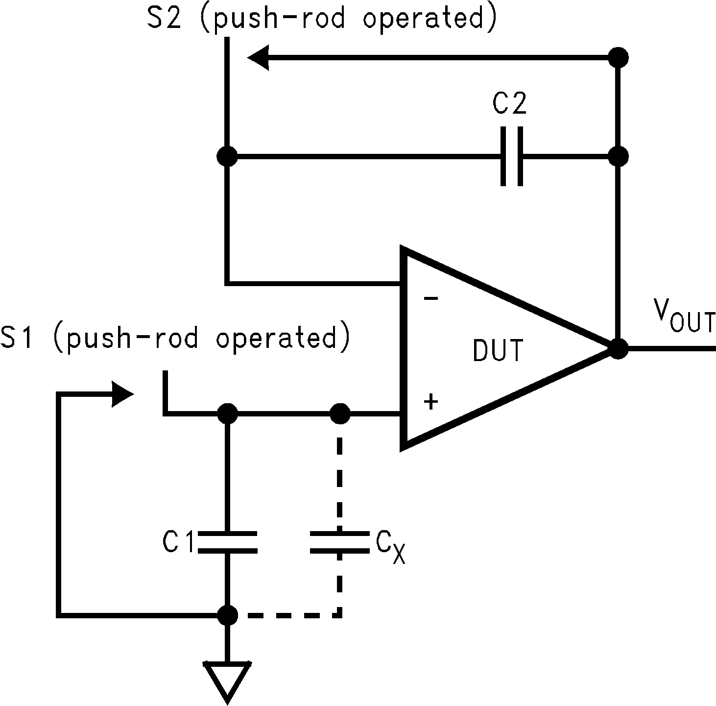
The test method of Figure 6-5 is appropriate for bench-testing bias current with reasonable accuracy. To understand the circuit operation, first close switch S2 momentarily. When S2 is opened, then:
 Figure 6-5 Simple Input Bias Current Test Circuit
A recommended capacitor for C2 is a 5pF or 10pF silver mica, NPO ceramic, or air-dielectric. When determining the magnitude of Ib−, take into account the leakage of the capacitor and socket. Leave switch S2 shorted most of the time, or else the dielectric absorption of the capacitor C2 can cause errors.
Similarly, if S1 is shorted momentarily (while leaving S2 shorted):
where Cx is the stray capacitance at the noninverting input.