SNLS558C April   2017  – May 2020 LMH0397

PRODUCTION DATA.  

  1. Features
  2. Applications
  3. Description
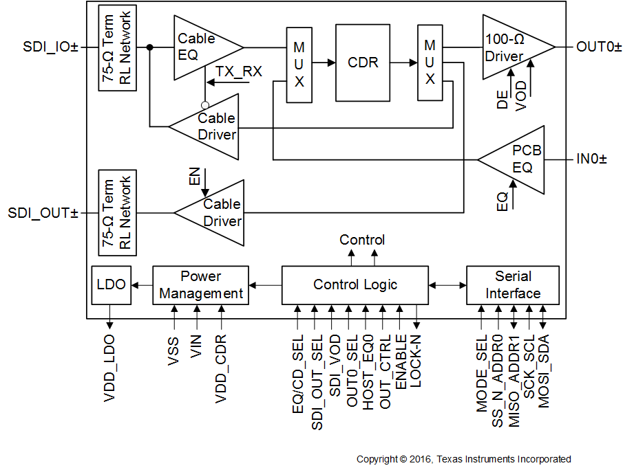
    1.     Simplified Block Diagram
  4. Revision History
  5. Description (continued)
  6. Pin Configuration and Functions
    1.     Pin Functions
  7. Specifications
    1. 7.1 Absolute Maximum Ratings
    2. 7.2 ESD Ratings
    3. 7.3 Recommended Operating Conditions
    4. 7.4 Thermal Information
    5. 7.5 Electrical Characteristics
    6. 7.6 Recommended SMBus Interface Timing Specifications
    7. 7.7 Serial Parallel Interface (SPI) Timing Specifications
    8. 7.8 Typical Characteristics
  8. Detailed Description
    1. 8.1 Overview
      1. 8.1.1 Equalizer Mode (EQ Mode)
      2. 8.1.2 Cable Driver Mode (CD Mode)
    2. 8.2 Functional Block Diagram
    3. 8.3 Feature Description
      1. 8.3.1  4-Level Input Pins and Thresholds
      2. 8.3.2  Equalizer (EQ) and Cable Driver (CD) Mode Control
        1. 8.3.2.1 EQ/CD_SEL Control
        2. 8.3.2.2 OUT0_SEL and SDI_OUT_SEL Control
      3. 8.3.3  Input Carrier Detect
      4. 8.3.4  –6-dB Splitter Mode Launch Amplitude for SDI_IO+ (EQ Mode Only)
      5. 8.3.5  Continuous Time Linear Equalizer (CTLE)
        1. 8.3.5.1 Line-Side Adaptive Cable Equalizer (SDI_IO+ in EQ Mode)
        2. 8.3.5.2 Host-Side Adaptive PCB Trace Equalizer (IN0± in CD Mode)
      6. 8.3.6  Clock and Data (CDR) Recovery
      7. 8.3.7  Internal Eye Opening Monitor (EOM)
      8. 8.3.8  Output Function Control
      9. 8.3.9  Output Driver Control
        1. 8.3.9.1 Line-Side Output Cable Driver (SDI_IO+ in CD Mode, SDI_OUT+ in EQ or CD Mode)
          1. 8.3.9.1.1 Output Amplitude (VOD)
          2. 8.3.9.1.2 Output Pre-Emphasis
          3. 8.3.9.1.3 Output Slew Rate
          4. 8.3.9.1.4 Output Polarity Inversion
        2. 8.3.9.2 Host-Side 100-Ω Output Driver (OUT0± in EQ or CD Mode)
      10. 8.3.10 Status Indicators and Interrupts
        1. 8.3.10.1 LOCK_N (Lock Indicator)
        2. 8.3.10.2 CD_N (Carrier Detect)
        3. 8.3.10.3 INT_N (Interrupt)
      11. 8.3.11 Additional Programmability
        1. 8.3.11.1 Cable EQ Index (CEI)
        2. 8.3.11.2 Digital MUTEREF
    4. 8.4 Device Functional Modes
      1. 8.4.1 System Management Bus (SMBus) Mode
        1. 8.4.1.1 SMBus Read and Write Transaction
          1. 8.4.1.1.1 SMBus Write Operation Format
          2. 8.4.1.1.2 SMBus Read Operation Format
      2. 8.4.2 Serial Peripheral Interface (SPI) Mode
        1. 8.4.2.1 SPI Read and Write Transactions
        2. 8.4.2.2 SPI Write Transaction Format
        3. 8.4.2.3 SPI Read Transaction Format
        4. 8.4.2.4 SPI Daisy Chain
    5. 8.5 Register Maps
  9. Application and Implementation
    1. 9.1 Application Information
      1. 9.1.1 SMPTE Requirements and Specifications
      2. 9.1.2 Low-Power Optimization in CD Mode
    2. 9.2 Typical Applications
      1. 9.2.1 Bidirectional I/O
        1. 9.2.1.1 Design Requirements
        2. 9.2.1.2 Detailed Design Procedure
        3. 9.2.1.3 Application Curves
      2. 9.2.2 Cable Equalizer With Loop-Through
        1. 9.2.2.1 Design Requirements
        2. 9.2.2.2 Detailed Design Procedure
        3. 9.2.2.3 Application Curves
  10. 10Power Supply Recommendations
  11. 11Layout
    1. 11.1 Layout Guidelines
      1. 11.1.1 Board Stack-Up and Ground References
      2. 11.1.2 High-Speed PCB Trace Routing and Coupling
        1. 11.1.2.1 SDI_IO± and SDI_OUT±
        2. 11.1.2.2 IN0± and OUT0±
      3. 11.1.3 Anti-Pads
      4. 11.1.4 BNC Connector Layout and Routing
      5. 11.1.5 Power Supply and Ground Connections
      6. 11.1.6 Footprint Recommendations
    2. 11.2 Layout Example
  12. 12Device and Documentation Support
    1. 12.1 Device Support
      1. 12.1.1 Developmental Support
    2. 12.2 Documentation Support
      1. 12.2.1 Related Documentation
    3. 12.3 Receiving Notification of Documentation Updates
    4. 12.4 Support Resources
    5. 12.5 Trademarks
    6. 12.6 Electrostatic Discharge Caution
    7. 12.7 Export Control Notice
    8. 12.8 Glossary
  13. 13Mechanical, Packaging, and Orderable Information
    1. 13.1 Package Option Addendum
      1. 13.1.1 Packaging Information
      2. 13.1.2 Tape and Reel Information

Package Options

Mechanical Data (Package|Pins)
Thermal pad, mechanical data (Package|Pins)
Orderable Information

Description

The LMH0397 is a 3G-SDI 75-Ω bidirectional I/O with integrated reclocker. This device can be configured either in input mode as an adaptive cable equalizer or in output mode as a dual cable driver, allowing system designers the flexibility to use a single BNC either as an input or output port to simplify HD-SDI video hardware designs. The integrated reclocker locks to all supported SMPTE data rates up to 2.97 Gbps in both modes. The bidirectional I/O has an on-chip 75-Ω termination and return loss compensation network that meets the stringent SMPTE return loss requirements.

An additional 75-Ω driver output allows the LMH0397 to support a variety of system functions. In EQ (Equalizer) Mode, this second 75-Ω driver can be used as a loop-through output. In Cable Driver (CD) Mode, this 75-Ω driver can be used as a second fan-out cable driver. The host-side 100-Ω driver can also be used as a loopback output in CD Mode for monitoring purposes.

Device Information(1)

PART NUMBER PACKAGE BODY SIZE (NOM)
LMH0397 WQFN (32) 5.00 mm × 5.00 mm
  1. For all available packages, see the orderable addendum at the end of the data sheet.

Simplified Block Diagram
LMH0397 front_page_block_diagram_lmh1297_snls545.gif