SNLS558C April   2017  – May 2020 LMH0397

PRODUCTION DATA.  

  1. Features
  2. Applications
  3. Description
    1.     Simplified Block Diagram
  4. Revision History
  5. Description (continued)
  6. Pin Configuration and Functions
    1.     Pin Functions
  7. Specifications
    1. 7.1 Absolute Maximum Ratings
    2. 7.2 ESD Ratings
    3. 7.3 Recommended Operating Conditions
    4. 7.4 Thermal Information
    5. 7.5 Electrical Characteristics
    6. 7.6 Recommended SMBus Interface Timing Specifications
    7. 7.7 Serial Parallel Interface (SPI) Timing Specifications
    8. 7.8 Typical Characteristics
  8. Detailed Description
    1. 8.1 Overview
      1. 8.1.1 Equalizer Mode (EQ Mode)
      2. 8.1.2 Cable Driver Mode (CD Mode)
    2. 8.2 Functional Block Diagram
    3. 8.3 Feature Description
      1. 8.3.1  4-Level Input Pins and Thresholds
      2. 8.3.2  Equalizer (EQ) and Cable Driver (CD) Mode Control
        1. 8.3.2.1 EQ/CD_SEL Control
        2. 8.3.2.2 OUT0_SEL and SDI_OUT_SEL Control
      3. 8.3.3  Input Carrier Detect
      4. 8.3.4  –6-dB Splitter Mode Launch Amplitude for SDI_IO+ (EQ Mode Only)
      5. 8.3.5  Continuous Time Linear Equalizer (CTLE)
        1. 8.3.5.1 Line-Side Adaptive Cable Equalizer (SDI_IO+ in EQ Mode)
        2. 8.3.5.2 Host-Side Adaptive PCB Trace Equalizer (IN0± in CD Mode)
      6. 8.3.6  Clock and Data (CDR) Recovery
      7. 8.3.7  Internal Eye Opening Monitor (EOM)
      8. 8.3.8  Output Function Control
      9. 8.3.9  Output Driver Control
        1. 8.3.9.1 Line-Side Output Cable Driver (SDI_IO+ in CD Mode, SDI_OUT+ in EQ or CD Mode)
          1. 8.3.9.1.1 Output Amplitude (VOD)
          2. 8.3.9.1.2 Output Pre-Emphasis
          3. 8.3.9.1.3 Output Slew Rate
          4. 8.3.9.1.4 Output Polarity Inversion
        2. 8.3.9.2 Host-Side 100-Ω Output Driver (OUT0± in EQ or CD Mode)
      10. 8.3.10 Status Indicators and Interrupts
        1. 8.3.10.1 LOCK_N (Lock Indicator)
        2. 8.3.10.2 CD_N (Carrier Detect)
        3. 8.3.10.3 INT_N (Interrupt)
      11. 8.3.11 Additional Programmability
        1. 8.3.11.1 Cable EQ Index (CEI)
        2. 8.3.11.2 Digital MUTEREF
    4. 8.4 Device Functional Modes
      1. 8.4.1 System Management Bus (SMBus) Mode
        1. 8.4.1.1 SMBus Read and Write Transaction
          1. 8.4.1.1.1 SMBus Write Operation Format
          2. 8.4.1.1.2 SMBus Read Operation Format
      2. 8.4.2 Serial Peripheral Interface (SPI) Mode
        1. 8.4.2.1 SPI Read and Write Transactions
        2. 8.4.2.2 SPI Write Transaction Format
        3. 8.4.2.3 SPI Read Transaction Format
        4. 8.4.2.4 SPI Daisy Chain
    5. 8.5 Register Maps
  9. Application and Implementation
    1. 9.1 Application Information
      1. 9.1.1 SMPTE Requirements and Specifications
      2. 9.1.2 Low-Power Optimization in CD Mode
    2. 9.2 Typical Applications
      1. 9.2.1 Bidirectional I/O
        1. 9.2.1.1 Design Requirements
        2. 9.2.1.2 Detailed Design Procedure
        3. 9.2.1.3 Application Curves
      2. 9.2.2 Cable Equalizer With Loop-Through
        1. 9.2.2.1 Design Requirements
        2. 9.2.2.2 Detailed Design Procedure
        3. 9.2.2.3 Application Curves
  10. 10Power Supply Recommendations
  11. 11Layout
    1. 11.1 Layout Guidelines
      1. 11.1.1 Board Stack-Up and Ground References
      2. 11.1.2 High-Speed PCB Trace Routing and Coupling
        1. 11.1.2.1 SDI_IO± and SDI_OUT±
        2. 11.1.2.2 IN0± and OUT0±
      3. 11.1.3 Anti-Pads
      4. 11.1.4 BNC Connector Layout and Routing
      5. 11.1.5 Power Supply and Ground Connections
      6. 11.1.6 Footprint Recommendations
    2. 11.2 Layout Example
  12. 12Device and Documentation Support
    1. 12.1 Device Support
      1. 12.1.1 Developmental Support
    2. 12.2 Documentation Support
      1. 12.2.1 Related Documentation
    3. 12.3 Receiving Notification of Documentation Updates
    4. 12.4 Support Resources
    5. 12.5 Trademarks
    6. 12.6 Electrostatic Discharge Caution
    7. 12.7 Export Control Notice
    8. 12.8 Glossary
  13. 13Mechanical, Packaging, and Orderable Information
    1. 13.1 Package Option Addendum
      1. 13.1.1 Packaging Information
      2. 13.1.2 Tape and Reel Information

Package Options

Mechanical Data (Package|Pins)
Thermal pad, mechanical data (Package|Pins)
Orderable Information

Typical Characteristics

TA = 25°C and VIN = VDD_CDR = 2.5 V (unless otherwise noted)
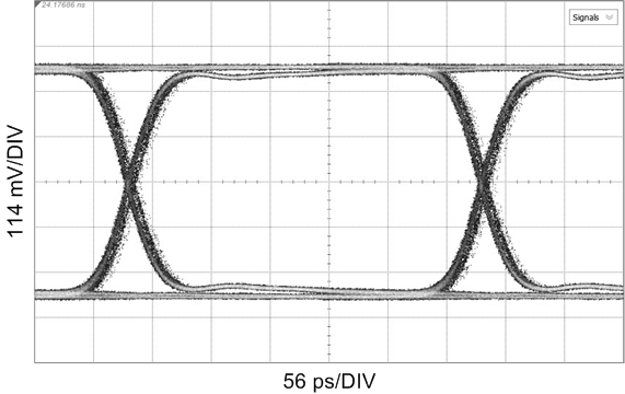
LMH0397 EQ_2.97G_200m_Reclocked_PRBS10_114mV_56ps.pngFigure 4. EQ Mode at 2.97 Gbps, Measured at OUT0±,
200-m Belden 1694A Before SDI_IO+
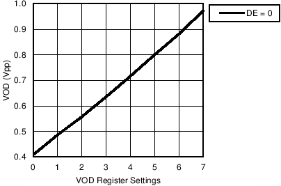
LMH0397 vod_vs_vod_reg.pngFigure 6. OUT0 VOD vs. OUT0 VOD and DE
Register Settings
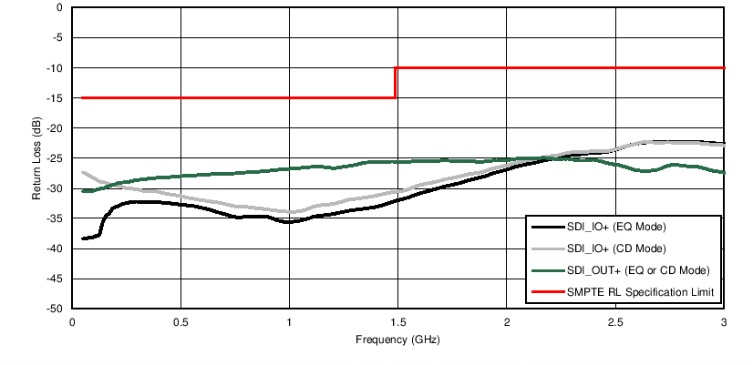
LMH0397 C001_SNLS558.png
Measured with LMH1297EVM
Figure 8. Return Loss (RL) vs Frequency
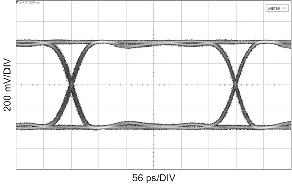
LMH0397 CD_IO_2.97G_PRBS10_200mV_56ps.pngFigure 5. CD Mode at 2.97 Gbps, Measured at SDI_IO+,
20-in. FR4 Before IN0±
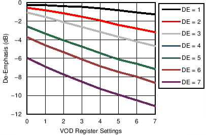
LMH0397 de_vs_de_vod.pngFigure 7. OUT0 De-Emphasis vs. OUT0 VOD and DE
Register Settings